ALLPCB


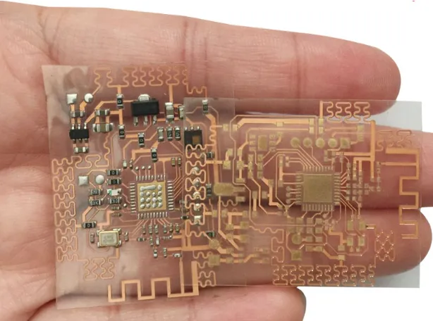
In the fast-evolving world of electronics, transparent flex PCBs (Printed Circuit Boards) are emerging as a groundbreaking solution for applications requiring both functionality and aesthetics. These flexible transparent circuits combine the benefits of flexibility with optical clarity, making them ideal for innovative designs in devices like foldable smartphones, wearable tech, and advanced displays. However, manufacturing these cutting-edge boards comes with unique hurdles, especially when adhering to industry standards like IPC-6013. In this blog, we’ll explore the innovations driving transparent flex PCBs, the material and manufacturing challenges they face, and how IPC-6013 standards impact their production. Let’s dive into the details to understand how these challenges shape the future of flexible transparent circuits.
What Are Transparent Flex PCBs and Why Do They Matter?
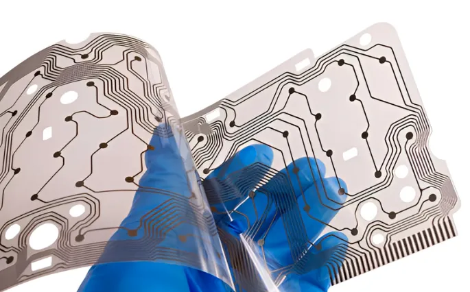
Transparent flex PCBs are a specialized type of flexible circuit board made from materials that allow light to pass through, offering both optical clarity and the ability to bend or fold. Unlike traditional rigid PCBs or even standard flex PCBs, these boards are designed for applications where visibility or aesthetics are critical, such as in smart glasses, transparent displays, or compact medical devices.
The significance of flexible transparent circuits lies in their ability to reduce light scattering and enhance device efficiency. For instance, in optical applications, a transparent PCB can improve light transmission by up to 90%, compared to traditional opaque boards that block light entirely. This makes them a game-changer for industries pushing the boundaries of design and functionality.
However, creating these innovative boards is no easy task. From selecting the right materials to meeting strict quality standards like IPC-6013 for transparent PCBs, manufacturers face a range of obstacles. Let’s break down the innovations and challenges in detail.
Innovations Driving Transparent Flex PCBs
The rise of transparent flex PCBs is fueled by several key innovations in materials, design, and manufacturing techniques. These advancements are pushing the boundaries of what’s possible in electronics design.
1. Advanced Transparent Materials
One of the biggest breakthroughs in flexible transparent circuits is the development of new materials like transparent polyimide (PI) and polyethylene terephthalate (PET). These materials offer high optical clarity, with light transmittance rates often exceeding 85%, while maintaining the flexibility needed for bending radii as tight as 1mm. They also provide excellent thermal stability, withstanding temperatures up to 200°C, which is critical for soldering and assembly processes.
2. Conductive Transparent Layers
Traditional copper traces are replaced or supplemented with transparent conductive materials like indium tin oxide (ITO) or silver nanowires in transparent flex PCBs. These materials maintain electrical conductivity while allowing light to pass through. For example, ITO layers can achieve sheet resistance as low as 10 ohms per square, ensuring efficient signal transmission in devices like touchscreens.
3. Miniaturization and Integration
Transparent flex PCBs enable greater miniaturization by allowing components to be embedded in compact, foldable designs. This is particularly valuable in wearable technology, where space is limited. Their ability to integrate seamlessly into curved or irregular shapes also enhances design freedom for engineers working on next-generation devices.
Understanding IPC-6013 Standards for Transparent Flex PCBs
IPC-6013 is the industry standard for the qualification and performance of flexible and rigid-flex printed boards. It provides guidelines on design, material selection, fabrication, and assembly to ensure quality and reliability. For transparent flex PCBs, adhering to IPC-6013 is critical but challenging due to their unique properties.
Key Aspects of IPC-6013 for Transparent PCBs
IPC-6013 outlines specific requirements that impact the production of flexible transparent circuits, including:
- Material Specifications: The standard defines acceptable materials for flexible circuits, emphasizing durability and performance under stress. For transparent PCBs, this means ensuring that materials like transparent polyimide meet tensile strength and thermal resistance criteria.
- Plating and Conductive Layers: IPC-6013 sets strict rules for plating thickness and adhesion, which can be tricky with transparent conductive materials like ITO that may have lower adhesion compared to copper.
- Quality and Testing: The standard requires rigorous testing for defects like delamination or cracking, which are more pronounced risks in transparent flex PCBs due to their thin, delicate nature.
Meeting these standards ensures that transparent flex PCBs are reliable for end-use applications, but it also adds complexity to the manufacturing process. Let’s explore the specific challenges tied to materials and production under IPC-6013 guidelines.
Material Challenges in Transparent Flex PCB Manufacturing
While the materials used in transparent flex PCBs enable their unique properties, they also introduce significant hurdles during design and production. Here are some of the key material challenges:
1. Limited Material Availability
Transparent substrates like clear polyimide or PET are not as widely available as standard flex PCB materials. Their production is specialized, often leading to higher costs and longer lead times. Additionally, not all transparent materials meet the mechanical and thermal requirements of IPC-6013, limiting options for manufacturers.
2. Fragility and Mechanical Stress
Transparent materials tend to be thinner and more brittle than standard flex substrates. For example, a typical transparent polyimide film may have a thickness of just 25 micrometers, making it prone to tearing or cracking during bending cycles. IPC-6013 mandates that flex circuits withstand a specific number of bend cycles (often thousands), which can be difficult to achieve with these delicate materials.
3. Compatibility with Conductive Layers
Transparent conductive materials like ITO or silver nanowires often struggle with adhesion to flexible substrates. Poor adhesion can lead to failures during assembly or use, violating IPC-6013 quality standards. Moreover, these materials may have higher resistance compared to copper, impacting signal integrity in high-speed applications where impedance control is critical (e.g., maintaining 50 ohms for RF signals).
Manufacturing Challenges for Flexible Transparent Circuits
Beyond material issues, the production process for transparent flex PCBs introduces its own set of challenges. These hurdles often stem from the need to balance optical clarity, flexibility, and compliance with IPC-6013 standards.
1. Precision in Fabrication
Manufacturing transparent flex PCBs requires extreme precision to avoid defects that could impair optical clarity. For instance, even minor scratches or contamination during etching can create visible flaws, rendering the board unusable for applications like displays. IPC-6013 requires strict control over fabrication processes, adding to the complexity and cost of production.
2. Thermal Management During Assembly
Transparent materials often have lower thermal resistance compared to standard flex substrates. During soldering, temperatures can exceed 260°C, risking deformation or discoloration of the transparent substrate. Manufacturers must use specialized low-temperature soldering techniques or adhesives to meet IPC-6013 assembly standards without damaging the board.
3. Testing and Inspection Difficulties
Inspecting transparent flex PCBs for defects is more challenging than with opaque boards. Traditional automated optical inspection (AOI) systems may struggle to detect issues like micro-cracks or delamination in transparent materials. IPC-6013 mandates thorough testing, often requiring advanced inspection tools or manual checks, which can slow down production and increase costs.
Overcoming Challenges with Design and Manufacturing Strategies
Despite the obstacles, there are practical strategies to address material and manufacturing challenges while meeting IPC-6013 standards for transparent flex PCBs. Here are some actionable approaches:
1. Material Selection and Testing
Engineers should prioritize materials with proven performance under IPC-6013 testing conditions. For instance, selecting a transparent polyimide with a high glass transition temperature (Tg) above 200°C can improve thermal stability during assembly. Conducting early material testing for bend cycles and adhesion can also prevent failures down the line.
2. Design Optimization
Design plays a crucial role in mitigating manufacturing challenges. Using larger bend radii (e.g., 3mm instead of 1mm) can reduce stress on fragile transparent materials. Additionally, incorporating teardrop vias and large annular rings, as recommended by industry guidelines, can enhance durability and signal reliability.
3. Advanced Manufacturing Techniques
Adopting cutting-edge fabrication methods, such as laser etching for precise trace patterns, can minimize damage to transparent substrates. Similarly, using adhesive-less materials or low-temperature bonding techniques can prevent thermal damage during assembly, ensuring compliance with IPC-6013 standards.
The Future of Transparent Flex PCBs
The potential for transparent flex PCBs is immense, with applications ranging from foldable electronics to advanced medical imaging devices. As material science and manufacturing technologies continue to advance, many of the current challenges tied to flexible transparent circuits are likely to be resolved. Innovations like stretchable transparent substrates or hybrid conductive materials could further expand their capabilities, while updates to standards like IPC-6013 may better accommodate these unique boards.
For now, engineers and manufacturers must navigate the delicate balance between innovation and practicality. By understanding the material and manufacturing challenges—and leveraging strategic design and production methods—it’s possible to create reliable, high-quality transparent flex PCBs that meet industry standards and push the boundaries of modern electronics.
Conclusion
Transparent flex PCBs represent a thrilling frontier in electronics, offering unmatched design flexibility and aesthetic appeal for cutting-edge devices. However, their production is fraught with challenges, from material fragility to stringent IPC-6013 requirements for transparent PCBs. By focusing on advanced materials, precise manufacturing, and optimized design, the industry can overcome these hurdles and unlock the full potential of flexible transparent circuits. Whether you’re an engineer or a product designer, staying informed about these innovations and challenges is key to harnessing the power of transparent flex PCBs in your next project.