 ALLPCB


In the world of electronics, Printed Circuit Boards (PCBs) are the backbone of almost every device. When a PCB fails, it can lead to costly downtime, product delays, or even safety hazards. For engineers, understanding how to identify and resolve these issues is critical. So, what are the top methods for PCB failure analysis? In this blog, we’ll dive into the top 5 PCB failure analysis methods that every engineer should master, covering PCB testing techniques, PCB inspection methods, advanced PCB analysis, and PCB fault finding strategies. Whether you’re troubleshooting a prototype or ensuring quality in mass production, these techniques will help you pinpoint problems and improve reliability.
Let’s explore these methods in detail, breaking down each approach with practical insights, actionable steps, and technical depth to support your work in electronics design and manufacturing.
Why PCB Failure Analysis Matters for Engineers
Before we dive into the specific methods, let’s understand why PCB failure analysis is so important. PCBs are complex systems with multiple layers, tiny traces, and countless components. A single failure—whether it’s a short circuit, open connection, or component breakdown—can halt an entire project. Effective PCB fault finding and analysis not only save time and money but also ensure the safety and performance of the final product. By mastering PCB testing techniques and inspection methods, engineers can prevent recurring issues, improve design quality, and maintain customer trust.
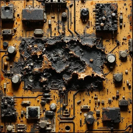
1. Visual Inspection: The First Step in PCB Fault Finding
Visual inspection is often the starting point for PCB failure analysis. It’s a simple yet effective method that requires minimal equipment—just a magnifying glass or a microscope in some cases. This PCB inspection method focuses on identifying obvious physical defects such as burnt components, broken traces, or poor soldering joints.
How to Perform Visual Inspection:
- Start by examining the PCB under good lighting with magnification if needed (10x to 20x is often sufficient for detailed checks).
- Look for discoloration, which might indicate overheating (often seen as brown or black spots on the board).
- Check for physical damage like cracks in the substrate or bulging capacitors, which can signal electrical stress or mechanical impact.
- Inspect solder joints for cold soldering (dull, uneven joints) or bridges that could cause shorts.
Why It’s Effective: Many PCB failures are visible to the trained eye. For instance, a burnt resistor or a cracked trace can be spotted without advanced tools, saving time before moving to complex PCB testing techniques. However, this method has limitations—it won’t detect internal layer issues or microscopic defects.
2. In-Circuit Testing (ICT): Precision PCB Testing Techniques
In-Circuit Testing (ICT) is a powerful method for PCB fault finding, especially during manufacturing or after assembly. ICT uses a bed-of-nails fixture to make contact with test points on the PCB, checking for shorts, opens, and component functionality without powering up the board in most cases.
How ICT Works:
- A custom test fixture connects to predefined test points on the PCB.
- The system measures resistance, capacitance, and other electrical parameters to verify component values (e.g., a resistor should read within ±5% of its rated value, such as 10 kΩ).
- It detects issues like incorrect component placement or soldering defects by comparing results against a known good board.
Benefits for Engineers: ICT is fast and highly accurate for high-volume production, catching up to 90% of assembly-related defects. For example, if a capacitor is installed backward, ICT can flag the issue by detecting an abnormal capacitance reading. However, it requires upfront investment in test fixtures and may not identify functional failures under real operating conditions.
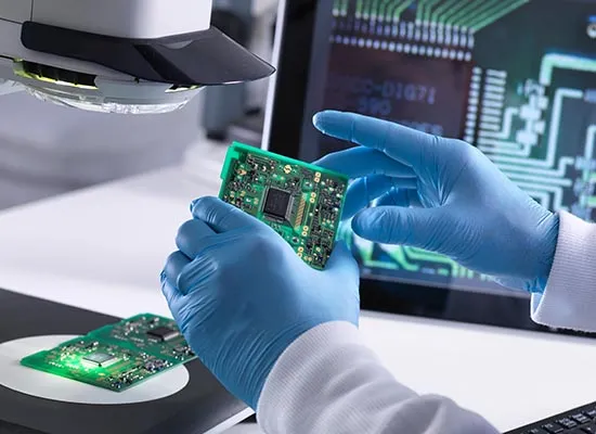
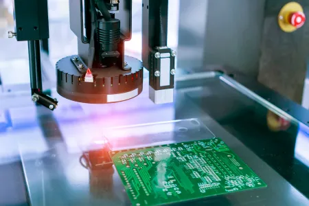
3. Automated Optical Inspection (AOI): Advanced PCB Inspection Methods
Automated Optical Inspection (AOI) is a non-contact, high-speed PCB inspection method that uses cameras and image processing software to detect defects. It’s widely used in manufacturing to spot issues like missing components, misalignments, or solder defects before the board moves to functional testing.
Key Features of AOI:
- High-resolution cameras scan the PCB surface, capturing images at multiple angles.
- Software compares the images to a reference design or golden board, flagging anomalies (e.g., a solder joint width deviating by more than 0.1 mm from the standard).
- It can inspect both surface-mount and through-hole components with precision.
Why Engineers Rely on AOI: AOI is ideal for catching visual defects that human inspectors might miss, especially on densely populated boards with components as small as 0402 (0.4 mm x 0.2 mm). It’s a critical step in advanced PCB analysis, reducing the risk of defective boards reaching the end user. However, AOI can’t detect electrical issues or internal layer problems, so it’s often paired with other methods.
4. X-Ray Inspection: Uncovering Hidden Defects in Advanced PCB Analysis
X-Ray inspection is a go-to method for advanced PCB analysis when internal defects are suspected. This non-destructive technique uses X-ray imaging to see through the PCB, revealing issues in internal layers, vias, and solder joints under components like Ball Grid Arrays (BGAs).
How X-Ray Inspection Helps with PCB Fault Finding:
- It detects voids in solder joints, which can weaken connections and cause failures (e.g., a void larger than 25% of the joint area is often considered a defect).
- It identifies misaligned or broken internal traces in multilayer boards, which are invisible to visual or AOI methods.
- It checks for hidden shorts or opens under components with fine pitch leads (e.g., 0.5 mm pitch BGAs).
Practical Use Case: Imagine a multilayer PCB failing intermittently due to a suspected via issue. X-Ray inspection can reveal a crack in the via barrel, allowing engineers to address the root cause—perhaps a manufacturing defect or thermal stress during soldering. While highly effective, X-Ray equipment is expensive and requires trained operators, making it less accessible for smaller projects.
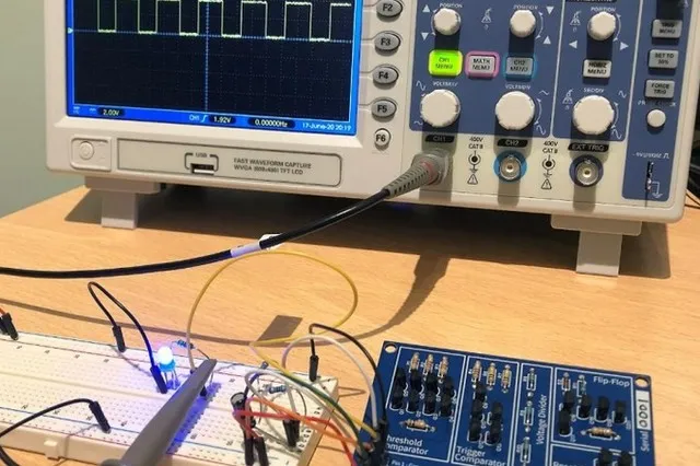
5. Functional Testing: Real-World PCB Testing Techniques
Functional testing is the ultimate step in PCB failure analysis, simulating real-world operating conditions to verify the board’s performance. Unlike ICT or AOI, which focus on assembly or physical defects, functional testing checks if the PCB works as intended in its final application.
Steps in Functional Testing:
- Power up the PCB and connect it to a test setup mimicking its end-use environment.
- Measure key parameters like signal integrity (e.g., ensuring a digital signal switches at 3.3V with a rise time under 5 ns) and current draw (e.g., confirming it’s within 10% of the design spec, such as 500 mA).
- Stress-test the board under extreme conditions like high temperature (up to 85°C) or voltage fluctuations to identify weak points.
Advantages for Engineers: Functional testing catches issues that other methods miss, such as firmware bugs or marginal components that fail only under load. For instance, a microcontroller might pass ICT but fail to boot due to a timing issue with a clock signal. The downside is that functional testing can be time-consuming and often requires custom test setups.
Combining Methods for Comprehensive PCB Failure Analysis
While each of these PCB failure analysis methods has unique strengths, the best results come from combining them. Start with visual inspection to catch obvious issues, then use AOI and ICT for assembly defects during production. For deeper issues, turn to X-Ray inspection, and finally, validate the board with functional testing. This layered approach ensures no defect goes unnoticed, whether it’s a visible crack or a hidden short.
For example, consider a PCB failing due to intermittent power issues. Visual inspection might show no obvious damage, but ICT could reveal a short circuit. X-Ray inspection might then pinpoint the short to a buried via, and functional testing confirms the board fails under load. By using multiple PCB testing techniques and inspection methods, you can systematically narrow down the root cause.
Tips for Effective PCB Fault Finding
To make the most of these PCB failure analysis methods, keep these tips in mind:
- Document Everything: Record observations, test results, and images at each step. This helps track patterns, especially for recurring failures.
- Use Design for Testability (DFT): Include test points and access to critical nets in your PCB layout to simplify ICT and functional testing.
- Analyze Failure Trends: If multiple boards fail in the same way (e.g., a specific trace breaking), investigate the design or manufacturing process for root causes like thermal stress or over-etching.
- Invest in Training: Ensure your team is skilled in advanced PCB analysis tools like X-Ray systems to avoid misdiagnosis.
Conclusion: Mastering PCB Failure Analysis for Better Designs
PCB failure analysis is a critical skill for engineers, ensuring that designs are reliable and products perform as expected. By mastering these top 5 methods—visual inspection, in-circuit testing, automated optical inspection, X-Ray inspection, and functional testing—you’ll be equipped to tackle any issue, from surface-level defects to complex internal faults. Each PCB testing technique and inspection method plays a vital role in the broader process of PCB fault finding and advanced PCB analysis.
Implementing these strategies not only helps resolve current failures but also prevents future ones, improving your design process and product quality. As technology evolves, staying updated on the latest tools and techniques will keep you ahead in the fast-paced world of electronics engineering. Start applying these methods today to build more robust and reliable PCBs.


