ALLPCB


If you're looking to ensure the quality and reliability of printed circuit boards (PCBs), understanding PCB inspection methods, equipment, checklists, and processes is essential. In this comprehensive guide, we'll walk you through the critical techniques and technologies used in PCB inspection, helping you achieve flawless results in electronics manufacturing. Whether you're an engineer, a manufacturer, or a quality control professional, this post will provide actionable insights to elevate your PCB production standards.
Why PCB Inspection Matters in Electronics Manufacturing
PCB inspection is a cornerstone of quality control in electronics manufacturing. A single defect in a PCB can lead to system failures, costly recalls, or compromised safety. By implementing robust inspection methods, manufacturers can catch issues early, reduce waste, and ensure that every board meets industry standards. With the complexity of modern electronics, such as multi-layer boards and high-density interconnects, thorough inspection isn't just an option—it's a necessity.
In this guide, we'll cover everything from basic visual checks to advanced automated technologies, ensuring you have the knowledge to maintain high-quality output. Let's start by exploring the core PCB inspection methods used in the industry.

Key PCB Inspection Methods for Quality Assurance
There are several proven PCB inspection methods that manufacturers rely on to detect defects and ensure functionality. Each method has its strengths and is often used at different stages of production. Here's a detailed look at the most common techniques.
1. Manual Visual Inspection (MVI)
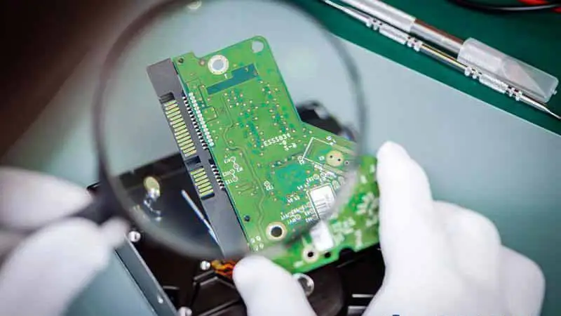
Manual visual inspection is the simplest and most accessible method for checking PCBs. It involves trained technicians examining boards with the naked eye or using basic tools like magnifying glasses or stereo microscopes. This method is ideal for spotting obvious defects such as misaligned components, soldering issues, or visible cracks.
While MVI is cost-effective, it has limitations. Human error can lead to missed defects, especially in complex boards with tiny components. It's best used for initial checks or small-scale production runs. For high-volume manufacturing, combining MVI with automated methods yields better results.
2. Automated Optical Inspection (AOI)
Automated Optical Inspection, or AOI, uses high-resolution cameras and image-processing software to scan PCBs for defects. This method can detect issues like missing components, incorrect placements, and solder joint problems with precision. AOI systems often operate at speeds of up to 100 square centimeters per second, making them ideal for high-speed production lines.
AOI is non-contact, meaning it won't damage delicate boards, and it provides consistent results compared to manual methods. However, it may struggle with hidden defects beneath components, requiring complementary techniques for full coverage.
3. X-Ray Inspection (AXI)
X-Ray Inspection, also known as Automated X-Ray Inspection (AXI), is a powerful method for examining internal structures of PCBs. It can detect hidden defects like voids in solder joints, misaligned vias, or issues in multi-layer boards. X-ray systems penetrate through materials, providing a detailed view of areas invisible to the naked eye or AOI cameras.
This method is particularly useful for inspecting Ball Grid Array (BGA) components, where solder joints are hidden under the package. While highly effective, X-ray equipment can be expensive, and the process is slower than AOI, often reserved for critical applications or final quality checks.
4. Flying Probe Testing
Flying Probe Testing uses movable test probes to check electrical connectivity on a PCB. This method is ideal for low-volume or prototype boards because it doesn't require custom test fixtures, unlike traditional bed-of-nails testing. Flying probes can test for open circuits, shorts, and component values with high accuracy, often achieving test coverage of over 95% on complex designs.
The downside is speed—flying probe testing is slower than other automated methods, making it less suitable for mass production. Still, its flexibility makes it a valuable tool in the PCB inspection process.
5. In-Circuit Testing (ICT)
In-Circuit Testing evaluates the functionality of individual components on an assembled PCB. Using a bed-of-nails fixture, ICT applies electrical signals to test for shorts, opens, and component performance. This method can measure resistance, capacitance, and other parameters with precision, often within tolerances of ±1%.
ICT is highly effective for detecting manufacturing defects but requires custom fixtures, which can be costly and time-consuming to design. It's best suited for high-volume production where the upfront investment pays off over time.

Essential PCB Inspection Equipment for Modern Manufacturing
Having the right PCB inspection equipment is just as important as choosing the right methods. Here's a breakdown of the tools and technologies that play a critical role in ensuring PCB quality.
1. Stereo Microscopes
Stereo microscopes are a staple for manual visual inspection. They provide 3D magnification, typically ranging from 10x to 40x, allowing inspectors to spot tiny defects like hairline cracks or solder bridges. These are affordable and widely used in smaller operations or for spot-checking.
2. AOI Systems
As mentioned earlier, AOI systems are automated machines equipped with high-resolution cameras and advanced software. Modern AOI equipment can process up to 150,000 components per hour, drastically reducing inspection time while maintaining accuracy. They are a must-have for large-scale PCB manufacturing.
3. X-Ray Machines
X-ray machines designed for PCB inspection use low-energy radiation to create detailed images of internal structures. These systems can detect defects as small as 0.1mm in solder joints, making them indispensable for high-reliability applications like aerospace or medical devices.
4. Flying Probe Testers
Flying probe testers consist of robotic arms with precision probes that contact test points on a PCB. Advanced models can perform up to 100 tests per minute, offering a balance of speed and flexibility for smaller production runs or prototype validation.
5. ICT Fixtures and Testers
In-Circuit Testing equipment includes custom fixtures tailored to specific PCB designs. These testers can handle complex boards with thousands of test points, ensuring comprehensive electrical validation. While the setup cost is high, the throughput in mass production justifies the investment.

A Comprehensive PCB Inspection Checklist for Flawless Results
To streamline the PCB inspection process, following a detailed checklist ensures no defect goes unnoticed. Below is a practical PCB inspection checklist that covers key aspects of quality control.
- Pre-Inspection Preparation: Verify design files against the fabricated board to ensure alignment. Check for correct component placement and orientation before detailed inspection begins.
- Visual Inspection: Look for surface-level issues like scratches, misaligned components, or poor soldering. Use magnification tools for small or intricate areas.
- Solder Joint Quality: Inspect solder joints for uniformity, voids, or bridges. Ensure joints meet industry standards for shape and size.
- Component Verification: Confirm that all components match the Bill of Materials (BOM). Check for correct values, polarities, and markings.
- Electrical Testing: Perform continuity tests to detect open circuits or shorts. Use ICT or flying probe testing for thorough electrical validation.
- Hidden Defect Detection: Use X-ray inspection for multi-layer boards or BGA components to identify internal issues like voids or misaligned vias.
- Functional Testing: Test the fully assembled board under operating conditions to ensure it performs as intended. Simulate real-world scenarios if possible.
- Documentation: Record all inspection findings, including defects and corrective actions. Maintain logs for traceability and future reference.
Using this checklist as a guide during the PCB inspection process helps maintain consistency and ensures that every board meets quality standards.

The PCB Inspection Process: Step-by-Step
Understanding the PCB inspection process is key to integrating it seamlessly into manufacturing workflows. Here's a step-by-step breakdown of how inspection typically unfolds in a production environment.
Step 1: Design Verification
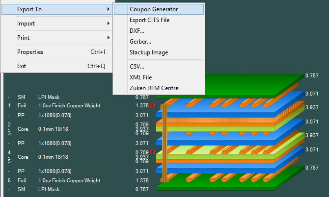
Before physical inspection begins, verify that the manufactured PCB matches the design files. This step often involves comparing Gerber files with the actual board layout to ensure no discrepancies exist.
Step 2: Initial Visual Check
Conduct a manual visual inspection to catch obvious defects. This quick check helps identify issues like missing components or visible damage before moving to automated methods.
Step 3: Automated Inspection
Use AOI systems to scan the board for surface-level defects. AOI can process large batches quickly, flagging areas that need closer attention. For hidden issues, employ X-ray inspection as needed.
Step 4: Electrical Testing
Perform electrical tests using flying probe or ICT equipment. This step ensures that all connections are intact and components function within specified parameters, such as resistance values within ±5% of the design spec.
Step 5: Functional Validation
Assemble the PCB into its intended system (if applicable) and test its performance under real-world conditions. This final step confirms that the board operates as expected before shipping.
Step 6: Reporting and Feedback
Document all findings and share feedback with the production team. Use data from inspections to improve future manufacturing processes, reducing defect rates over time.
While PCB inspection is critical, it's not without challenges. Miniaturization of components, for instance, makes defects harder to detect, requiring advanced equipment like high-resolution AOI or X-ray systems. Additionally, high-mix, low-volume production can strain resources, as frequent setup changes slow down inspection.
To address these issues, invest in versatile tools like flying probe testers that adapt to different board designs without custom fixtures. Also, train staff regularly to keep up with evolving technologies and standards. Combining multiple inspection methods ensures comprehensive coverage, even for the most complex boards.
Advancements in PCB Inspection Technologies
The field of PCB inspection is evolving rapidly, with new technologies enhancing accuracy and efficiency. Artificial Intelligence (AI) is now being integrated into AOI systems, enabling machines to learn from past inspections and reduce false positives by up to 30%. Additionally, 3D AOI systems provide depth analysis, improving detection of defects on uneven surfaces.
Another exciting development is the use of thermal imaging to identify overheating components during functional testing. This non-invasive method can spot potential failures before they occur, adding an extra layer of reliability to the inspection process.
Conclusion: Building Quality into Every PCB
Mastering PCB inspection methods, equipment, checklists, and processes is the key to delivering high-quality, reliable electronics. From manual visual checks to cutting-edge X-ray and AI-driven systems, each technique plays a vital role in catching defects and ensuring performance. By following a structured PCB inspection process and leveraging the right tools, manufacturers can minimize risks and build trust with their clients.
At ALLPCB, we're committed to supporting your journey toward flawless PCB production. Whether you're scaling up manufacturing or refining prototypes, integrating these inspection strategies will help you achieve consistent, high-quality results. Keep this guide handy as a reference, and take your PCB quality control to the next level.