 ALLPCB


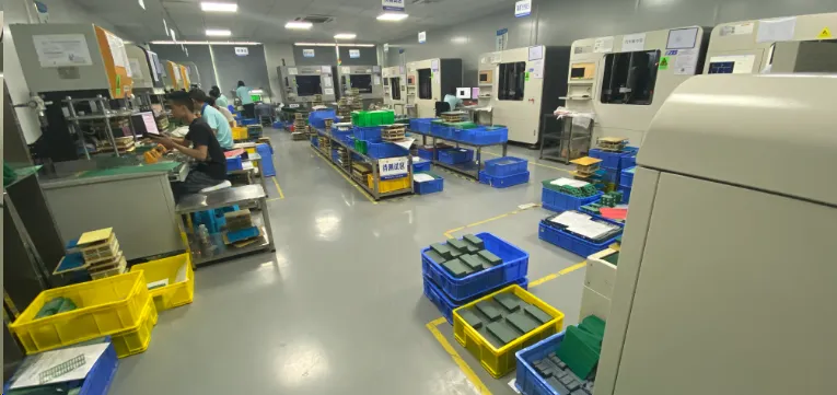
In the fast-paced world of electronics, ensuring the reliability of printed circuit boards (PCBs) during mass production is critical. How do manufacturers guarantee that every PCB meets high-quality standards? The answer lies in rigorous testing methods designed for mass production. From automated optical inspection (AOI) to in-circuit testing (ICT), functional testing, and flying probe testing, these PCB testing methods for mass production help catch defects early, reduce costs, and ensure that end products perform as expected. In this comprehensive guide, we’ll dive deep into these techniques, exploring how they contribute to PCB reliability and why they are essential for large-scale manufacturing.
Why PCB Testing Matters in Mass Production
PCBs are the backbone of nearly every electronic device, from smartphones to industrial machinery. A single defect in a PCB can lead to device failure, costly recalls, or even safety hazards. During mass production, where thousands or millions of boards are produced, the stakes are even higher. Testing isn’t just a final step; it’s an integral part of the manufacturing process that ensures quality and reliability at scale.
Without proper testing, issues like short circuits, open connections, or incorrect component placement can slip through, leading to significant losses. For instance, a study in the electronics industry found that undetected PCB defects can increase production costs by up to 30% due to rework and scrap. That’s why advanced PCB testing methods for mass production are non-negotiable for manufacturers aiming to deliver flawless products.
Key PCB Testing Methods for Mass Production
To achieve consistent quality in high-volume manufacturing, several testing methods are employed. Each method targets specific types of defects and fits different stages of the production process. Below, we explore the most widely used techniques, including automated optical inspection (AOI) for PCBs, in-circuit testing (ICT), functional testing, and flying probe testing for PCBs.
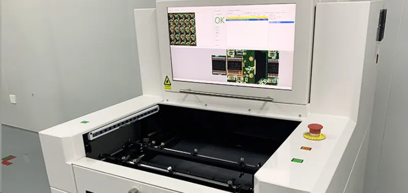
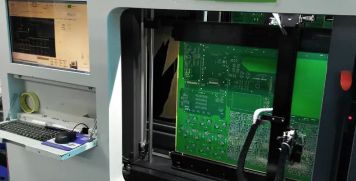
1. Automated Optical Inspection (AOI) for PCBs
Automated Optical Inspection, or AOI, is a cornerstone of PCB testing in mass production. This non-contact method uses high-resolution cameras and advanced image processing software to visually inspect PCBs for defects. AOI systems scan the board’s surface to detect issues like missing components, incorrect placements, soldering defects, and even tiny scratches or cracks that could affect performance.
How AOI Works: During inspection, the PCB is illuminated with specific lighting (often LED) to highlight features. Cameras capture detailed images, which are then compared to a reference design or “golden board.” Any deviation, such as a misplaced resistor or a solder bridge, triggers an alert for further review. Modern AOI systems can inspect hundreds of boards per hour, making them ideal for high-speed production lines.
Benefits for Mass Production: AOI is fast, accurate, and can detect defects early in the assembly process, often right after soldering. This reduces the risk of defective boards moving further down the line. For example, AOI can achieve defect detection rates of over 95%, significantly lowering the chances of faulty products reaching customers.
Limitations: While AOI excels at surface-level inspections, it cannot test electrical functionality or detect hidden defects like internal layer issues. That’s where other methods come in.
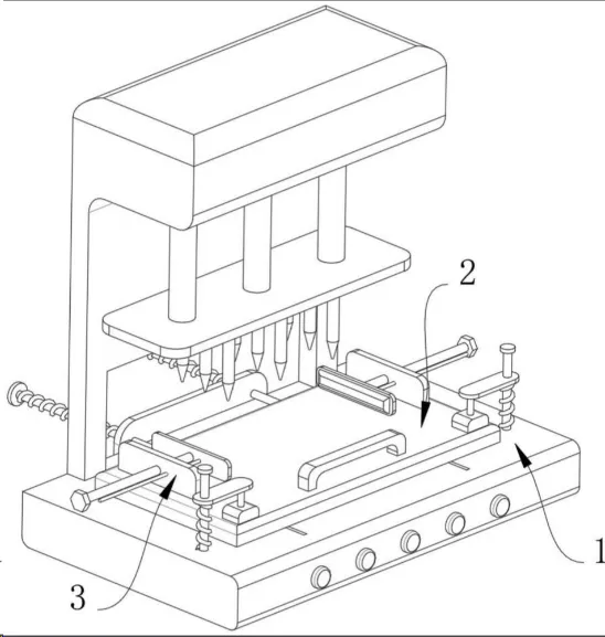
2. In-Circuit Testing (ICT) for PCBs
In-Circuit Testing, commonly known as ICT, is a powerful method for verifying the electrical performance of individual components on a PCB. Unlike AOI, which focuses on visual defects, ICT checks for issues like short circuits, open circuits, and incorrect component values by directly probing the board’s test points.
How ICT Works: ICT uses a custom fixture, often called a “bed of nails,” equipped with multiple probes that make contact with specific points on the PCB. These probes measure resistance, capacitance, and other electrical properties to ensure each component functions correctly. For instance, ICT can confirm that a resistor has the correct value, say 10 kΩ, within a tolerance of ±1%.
Benefits for Mass Production: ICT is highly accurate and can test hundreds of points on a board in seconds, making it suitable for large-scale manufacturing. It’s particularly effective for detecting manufacturing defects before functional testing. In a typical production run, ICT can reduce defect rates by catching up to 90% of electrical issues early.
Limitations: The main drawback of ICT is the need for a custom fixture, which can be expensive and time-consuming to design for each PCB layout. This makes ICT less flexible for low-volume runs or frequent design changes.
3. Functional Testing for PCBs
Functional testing takes PCB evaluation to the next level by simulating real-world operating conditions. This method tests the board as a complete system, ensuring it performs its intended function. For example, if the PCB is part of a power supply, functional testing might involve applying input voltages (e.g., 12V DC) and measuring output stability under various loads.
How Functional Testing Works: The PCB is connected to a test setup that mimics its final application. Test signals are applied, and the board’s responses are measured against expected outcomes. This could include checking signal integrity at high frequencies, such as 1 GHz for communication boards, or verifying that all LEDs on a control panel light up as expected.
Benefits for Mass Production: Functional testing ensures that the PCB works as a whole, catching issues that AOI or ICT might miss, such as firmware errors or integration problems. It’s often the final step before shipping, providing a last line of defense against defects.
Limitations: Functional testing can be time-consuming and may require custom test setups, especially for complex boards. It’s also typically performed on a sample basis rather than every board due to time constraints in mass production.
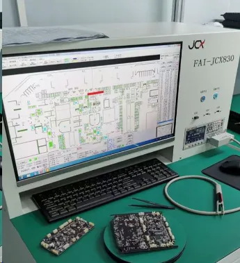
4. Flying Probe Testing for PCBs
Flying probe testing is a flexible and fixtureless alternative to ICT, ideal for both prototyping and smaller production runs within mass manufacturing workflows. Instead of a fixed bed of nails, flying probe systems use movable probes that dynamically contact test points on the PCB, guided by precise software.
How Flying Probe Testing Works: Two or more robotic probes move across the board, making contact with test points to measure electrical properties like resistance or continuity. For example, a probe might check for an open circuit between two pads or verify a capacitor’s value at 100 μF. The system’s software maps the board’s layout to guide the probes with pinpoint accuracy.
Benefits for Mass Production: Flying probe testing eliminates the need for custom fixtures, reducing setup costs and lead times. It’s especially useful for quick-turn projects or when testing a subset of boards during mass production. It can achieve test coverage of up to 85% of electrical connections without the overhead of ICT fixtures.
Limitations: Flying probe testing is slower than ICT because the probes move sequentially rather than testing multiple points simultaneously. This makes it less practical for very high-volume runs where speed is critical.
Comparing PCB Testing Methods for Mass Production
Each testing method has unique strengths and is best suited for specific scenarios in mass production. Here’s a quick comparison to help understand their roles:
- AOI for PCBs: Best for early-stage visual defect detection; fast and cost-effective but limited to surface issues.
- ICT for PCBs: Ideal for detailed electrical testing; highly accurate but requires custom fixtures.
- Functional Testing for PCBs: Ensures overall performance; critical for final validation but time-intensive.
- Flying Probe Testing for PCBs: Offers flexibility without fixtures; great for smaller runs or design changes but slower than ICT.
In practice, manufacturers often combine these methods to achieve comprehensive coverage. For instance, AOI might be used post-soldering, followed by ICT for electrical checks, and finally functional testing on a sample of finished boards.
Best Practices for Implementing PCB Testing in Mass Production
To maximize the effectiveness of PCB testing methods in mass production, manufacturers should follow these best practices:
- Design for Testability (DFT): Incorporate test points and accessible pads during the design phase to facilitate ICT and flying probe testing. Ensure components are spaced to allow probe access.
- Integrate Testing Early: Use AOI immediately after soldering to catch defects before additional assembly steps add cost to rework.
- Balance Speed and Coverage: For high-volume runs, prioritize fast methods like AOI and ICT for full testing, while using functional testing on representative samples.
- Regular Calibration: Maintain testing equipment through regular calibration to ensure accuracy. For example, AOI cameras should be checked for alignment to avoid false positives.
- Data-Driven Improvements: Analyze test data to identify recurring defects and address root causes in design or assembly processes.
By adopting these practices, manufacturers can streamline testing workflows, reduce defect rates, and improve overall PCB reliability.
Challenges in PCB Testing for Mass Production
Despite the advancements in testing technology, challenges remain in mass production environments:
- Complexity of Designs: Modern PCBs often feature high-density layouts with components as small as 0201 (0.2mm x 0.1mm), making testing more difficult.
- Cost Constraints: Comprehensive testing adds to production costs, especially for ICT fixtures or extensive functional testing setups.
- Time Pressures: High-volume production demands rapid testing, which can sometimes compromise thoroughness if not managed properly.
Addressing these challenges requires a strategic approach, balancing cost, time, and quality through the right mix of testing methods.
The Future of PCB Testing in Mass Production
As electronics continue to evolve, so do PCB testing technologies. Emerging trends include the integration of artificial intelligence (AI) in AOI systems to improve defect detection accuracy beyond 98%. Additionally, advancements in X-ray inspection are enhancing the ability to detect hidden defects in multi-layer boards. Automated testing systems are also becoming more interconnected, allowing real-time data sharing across production lines to optimize processes.
These innovations promise to make PCB testing faster, more accurate, and more cost-effective, ensuring that even the most complex boards meet stringent reliability standards in mass production.
Conclusion: Building Reliability Through Testing
Ensuring PCB reliability in mass production is a multi-step process that relies on a combination of advanced testing methods. Automated optical inspection (AOI) for PCBs catches visual defects early, in-circuit testing (ICT) verifies electrical integrity, functional testing confirms real-world performance, and flying probe testing offers flexibility for varied production needs. By strategically implementing these PCB testing methods for mass production, manufacturers can minimize defects, reduce costs, and deliver high-quality products that meet customer expectations.
At ALLPCB, we are committed to leveraging cutting-edge testing techniques to ensure every board we produce performs flawlessly. Whether you’re scaling up production or refining a prototype, understanding and applying these testing methods is the key to success in today’s competitive electronics market.


