ALLPCB


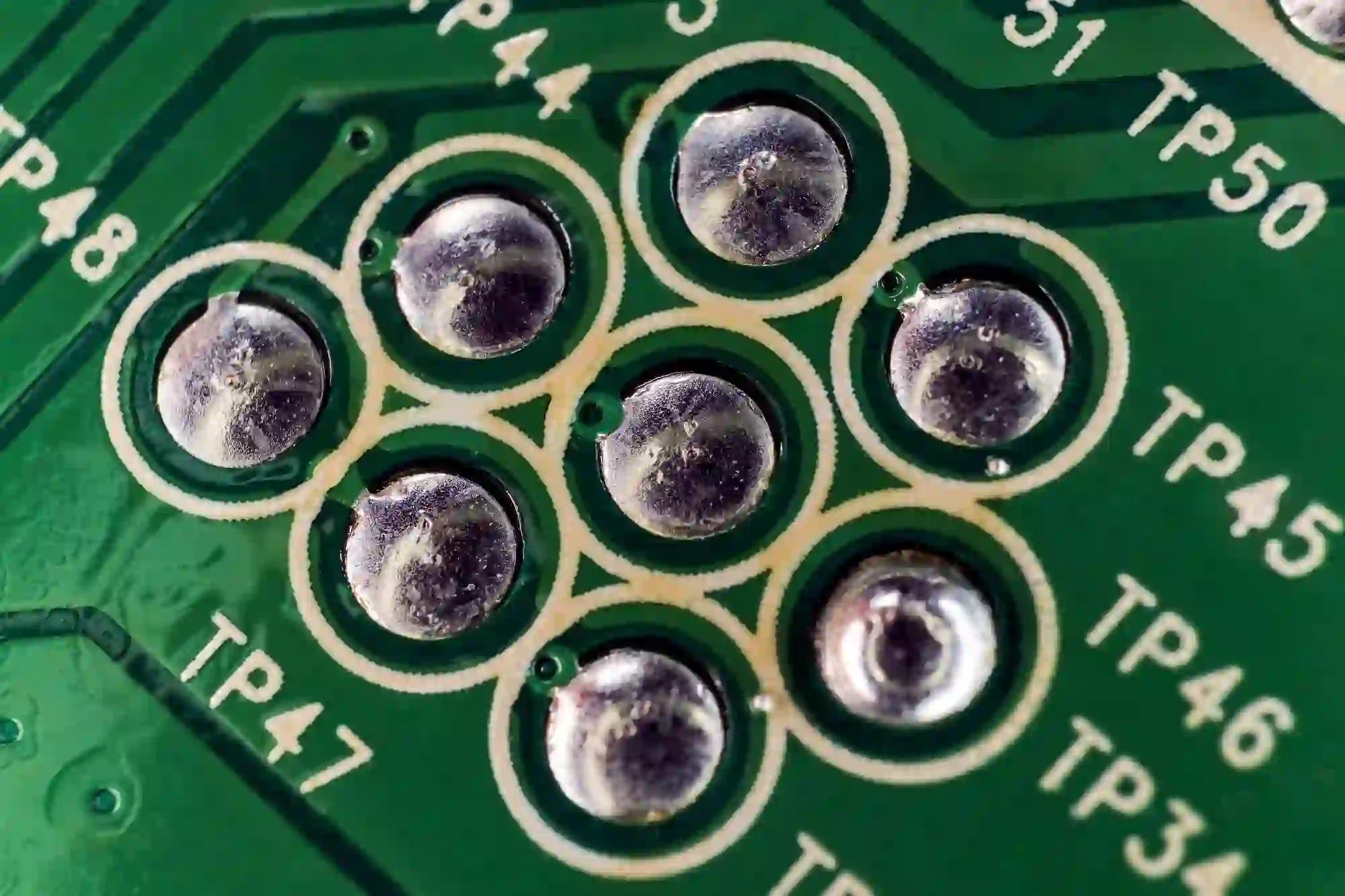
If you're an electrical engineer dealing with solder joint failures, you might be wondering what causes solder joint embrittlement and how to prevent it. Simply put, solder joint embrittlement is a condition where solder connections become brittle and prone to cracking due to factors like intermetallic compound formation, often involving materials like gold or palladium. This can weaken the joint and lead to reliability issues in electronic assemblies. In this blog, we'll dive deep into the causes, including gold embrittlement and palladium embrittlement in solder joints, explore prevention strategies, and review key industry standards to help you ensure robust connections.
Introduction to Solder Joint Embrittlement
Solder joints are the backbone of electronic assemblies, connecting components to printed circuit boards (PCBs). However, when these joints become brittle, they can fail under stress, leading to costly repairs or product failures. Solder joint embrittlement is a critical concern for electrical engineers working on high-reliability applications like aerospace, automotive, and medical devices. Understanding the mechanisms behind this issue—whether it's caused by gold, palladium, or other factors—is the first step to preventing it.
In this post, we'll break down the causes of solder joint embrittlement, focusing on specific mechanisms like gold embrittlement in solder joints and palladium embrittlement in solder joints. We'll also provide actionable solutions for preventing solder joint embrittlement and highlight relevant industry standards that guide best practices. Whether you're designing a new PCB or troubleshooting an existing assembly, this guide will equip you with the knowledge to tackle embrittlement head-on.
What Causes Solder Joint Embrittlement?
Before we can solve the problem, we need to understand what triggers solder joint embrittlement. This issue often arises when certain materials or conditions lead to the formation of brittle intermetallic compounds (IMCs) at the joint interface. Let's explore the primary causes, focusing on specific keywords like solder joint embrittlement causes.
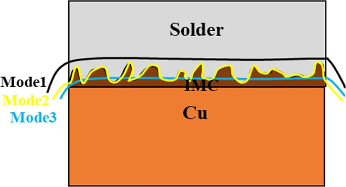
1. Formation of Intermetallic Compounds (IMCs)
IMCs form when solder alloys, typically tin-based, react with metals on the PCB or component leads, such as copper, nickel, gold, or palladium. While a thin layer of IMCs is necessary for a strong bond, excessive growth can make the joint brittle. For instance, in a tin-lead solder joint on a copper pad, the formation of Cu6Sn5 and Cu3Sn layers is normal. However, if these layers grow thicker over time—especially under high temperatures—they can reduce the joint's ductility, leading to cracks under thermal or mechanical stress.
Related Reading: Immersion Tin Thickness: What's the Ideal Specification for Reliable Solder Joints?
2. Gold Embrittlement in Solder Joints
Gold plating is commonly used on PCB pads and component leads to prevent oxidation and ensure good solderability. However, gold can cause significant issues, often referred to as gold embrittlement in solder joints. When gold dissolves into the solder during the soldering process, it forms brittle intermetallic compounds like AuSn4. If the gold content in the solder joint exceeds 3-5% by weight, the joint becomes prone to cracking, especially under vibration or thermal cycling.
For example, studies have shown that in a typical surface-mount technology (SMT) process, a gold layer thicker than 50 microinches (1.27 micrometers) can contribute to excessive AuSn4 formation, weakening the joint. This is a common issue in high-reliability applications where gold plating is thicker to ensure long-term corrosion resistance.
3. Palladium Embrittlement in Solder Joints
Similar to gold, palladium is often used in surface finishes like Electroless Nickel Immersion Gold (ENIG) with a palladium layer. While palladium offers excellent corrosion resistance, it can also lead to palladium embrittlement in solder joints. During soldering, palladium reacts with tin to form PdSn4 intermetallics, which are brittle and reduce the joint's mechanical strength. Although less common than gold embrittlement, palladium-related issues are still a concern, especially in fine-pitch components where even small weaknesses can cause failures.
4. Thermal and Mechanical Stress
Beyond material interactions, environmental factors play a big role in embrittlement. Thermal cycling—where a device experiences repeated heating and cooling—can cause stress due to differences in the coefficient of thermal expansion (CTE) between the solder, component, and PCB. For instance, a CTE mismatch between a ceramic capacitor (CTE of ~7 ppm/°C) and a FR-4 PCB (CTE of ~14-17 ppm/°C) can induce shear stress in the solder joint, accelerating crack formation in already brittle areas.
Mechanical stress, such as vibration in automotive electronics, can also exacerbate embrittlement. If the joint is already weakened by IMCs, even minor shocks can lead to failure.
Mechanisms Behind Solder Joint Embrittlement
Now that we’ve covered the causes, let’s dive deeper into the mechanisms that drive embrittlement. Understanding these processes at a microscopic level can help engineers design better assemblies.
1. Diffusion and IMC Growth
During soldering, atoms from the solder and the base metal diffuse into each other, forming IMCs at the interface. Over time, especially under elevated temperatures, these compounds continue to grow. For gold-plated surfaces, the diffusion of gold into tin-based solder is rapid, leading to a thick AuSn4 layer. This layer has poor mechanical properties, with a tensile strength significantly lower than the surrounding solder, making it a weak point.
2. Phase Transformation
In some cases, the solder itself undergoes phase changes that contribute to embrittlement. For example, in lead-free solders like SAC305 (Sn-3.0Ag-0.5Cu), the tin matrix can transform into different crystal structures under stress or aging, reducing ductility. This is often accelerated by the presence of contaminants or alloying elements from surface finishes.
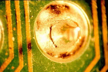
3. Crack Propagation
Once a solder joint is embrittled, even small stresses can initiate microcracks at the IMC layer. These cracks propagate through the joint, often following the brittle intermetallic boundaries. In high-reliability testing, such as thermal cycling from -55°C to 125°C (as per IPC standards), crack propagation can lead to complete joint failure within hundreds of cycles if embrittlement is severe.
Solutions for Preventing Solder Joint Embrittlement
With a clear understanding of solder joint embrittlement causes, let’s explore practical solutions for preventing solder joint embrittlement. These strategies are tailored for electrical engineers looking to improve the reliability of their designs.
1. Control Gold and Palladium Thickness
One of the most effective ways to mitigate gold and palladium embrittlement is to control the thickness of these layers on PCB pads and component leads. For gold, the industry often recommends a thickness of less than 5 microinches (0.127 micrometers) for immersion gold finishes like ENIG to minimize AuSn4 formation. If thicker gold is required for corrosion resistance, consider using a barrier layer of nickel to limit gold diffusion into the solder.
For palladium, similar guidelines apply. Opt for finishes with minimal palladium content or use alternative surface finishes like Organic Solderability Preservative (OSP) for low-risk applications.
2. Use Compatible Solder Alloys
Choosing the right solder alloy can reduce embrittlement risks. For instance, lead-free solders with lower silver content (e.g., Sn-0.7Cu instead of SAC305) form fewer brittle IMCs with gold and palladium. Additionally, some alloys are designed with additives to slow IMC growth, improving long-term reliability.
3. Optimize Soldering Processes
Adjusting the soldering temperature and time can limit the dissolution of gold or palladium into the solder. For example, using a reflow profile with a peak temperature of 240°C instead of 260°C for SAC305 solder can reduce gold diffusion by up to 20%, according to some studies. Shorter dwell times above liquidus also help minimize IMC formation.
Related Reading: Improving Solder Joint Quality in PCB Wave Soldering: A Step-by-Step Approach
4. Implement Design Improvements
Design your PCB and component layout to minimize thermal and mechanical stress. Use components with CTE values closer to the PCB material, or add underfill materials to absorb stress in high-risk areas. For vibration-heavy applications, consider conformal coatings to dampen mechanical shocks.
Industry Standards for Solder Joint Embrittlement
To ensure reliability, the electronics industry has established guidelines and standards related to solder joint embrittlement standards. Familiarity with these standards can help engineers design and manufacture robust assemblies.
1. IPC Standards
The Institute of Printed Circuits (IPC) provides several standards relevant to solder joint reliability:
- IPC-A-610: This standard outlines acceptability criteria for electronic assemblies, including solder joint appearance and defects like cracks due to embrittlement. It specifies that gold content in solder joints should not exceed 3% by weight to avoid embrittlement risks.
- IPC J-STD-001: This standard covers soldering requirements and emphasizes controlling surface finish thickness to prevent issues like gold or palladium embrittlement.
2. JEDEC Standards
JEDEC (Joint Electron Device Engineering Council) standards, such as JESD22-B102, provide test methods for evaluating solderability and joint reliability under thermal and mechanical stress. These tests help identify embrittlement issues during product qualification.
3. MIL-STD Specifications
For military and aerospace applications, MIL-STD-883 includes test methods for microelectronics, covering thermal cycling and vibration testing to detect solder joint failures caused by embrittlement. These standards often require stricter controls on gold and palladium content compared to commercial applications.
Case Studies and Real-World Applications
Let’s look at a couple of examples where solder joint embrittlement posed challenges and how engineers addressed them.
Case 1: Aerospace Electronics Failure
In an aerospace project, a batch of PCBs with ENIG finish experienced solder joint failures during thermal cycling tests (-55°C to 125°C, 1000 cycles). Analysis revealed excessive gold content (over 5% by weight) in the joints due to a thick immersion gold layer. The solution was to switch to a thinner gold layer (3 microinches) and introduce a nickel barrier, resulting in a 90% reduction in failure rates during subsequent testing.
Case 2: Automotive Sensor Cracking
An automotive sensor assembly showed joint cracking under vibration testing, attributed to palladium embrittlement from a Pd-containing finish. Engineers replaced the finish with OSP and adjusted the solder alloy to Sn-0.7Cu, significantly improving joint durability without compromising solderability.
Conclusion: Building Reliable Solder Joints
Solder joint embrittlement is a complex issue, but with the right knowledge and strategies, electrical engineers can minimize its impact. By understanding solder joint embrittlement causes like gold and palladium intermetallics, implementing solutions for preventing solder joint embrittlement, and adhering to solder joint embrittlement standards from IPC and JEDEC, you can design and manufacture reliable electronic assemblies.
Start by reviewing your PCB surface finishes and soldering processes. Limit gold and palladium thickness, choose compatible solder alloys, and optimize your reflow profiles. Additionally, leverage industry standards to guide your testing and quality control efforts. With these steps, you'll be well-equipped to tackle embrittlement and ensure long-lasting solder joints in your projects.
Have you encountered solder joint embrittlement in your work? Share your experiences or questions in the comments below—we'd love to hear from you!