 ALLPCB


In the world of printed circuit board (PCB) manufacturing, every detail counts when it comes to streamlining assembly and minimizing errors. One often-overlooked aspect is silkscreen design. A well-thought-out silkscreen can significantly boost PCB assembly efficiency by providing clear guidance during both manual and automated processes. In this comprehensive guide, we’ll explore how silkscreen markings for component polarity, silkscreen reference designator placement, and silkscreen aids for manual assembly can make a big difference in your production workflow. Let’s dive into the details of optimizing silkscreen design for better results.
What Is PCB Silkscreen and Why Does It Matter?
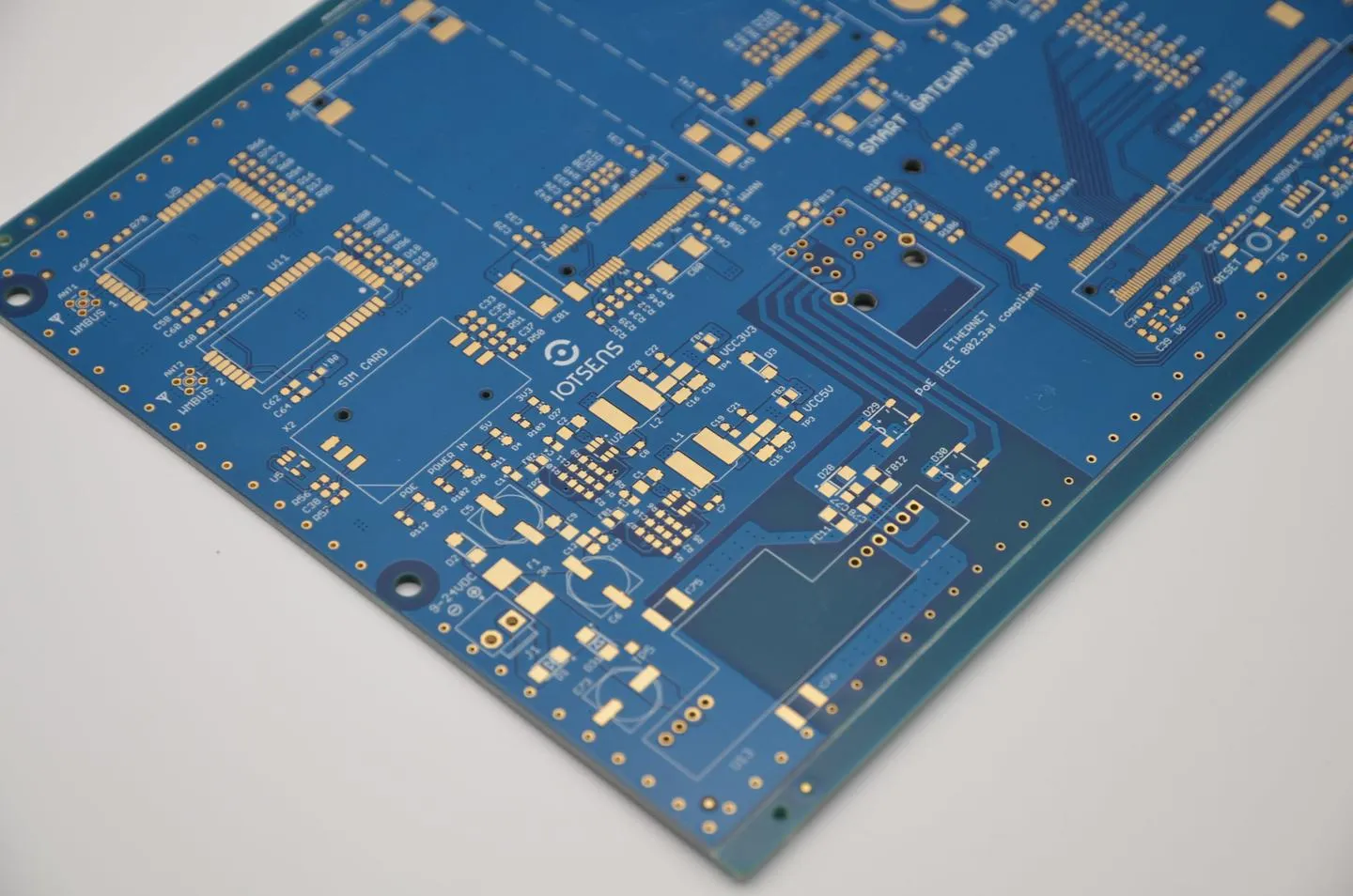
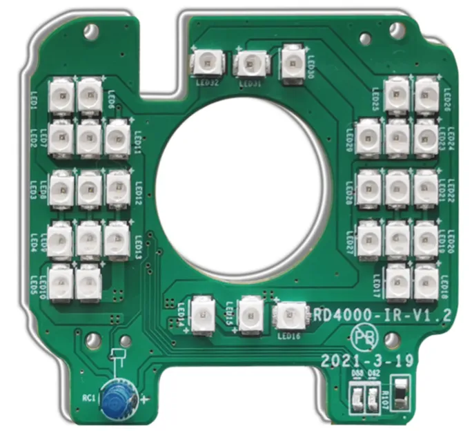
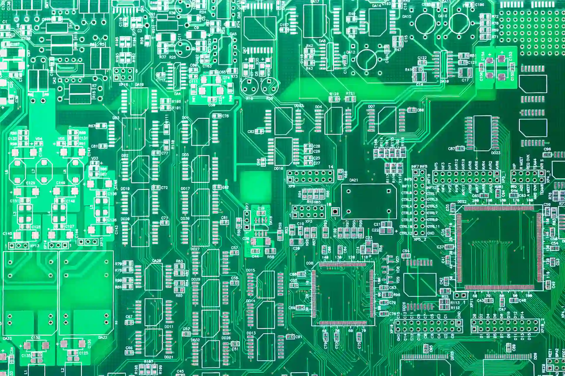
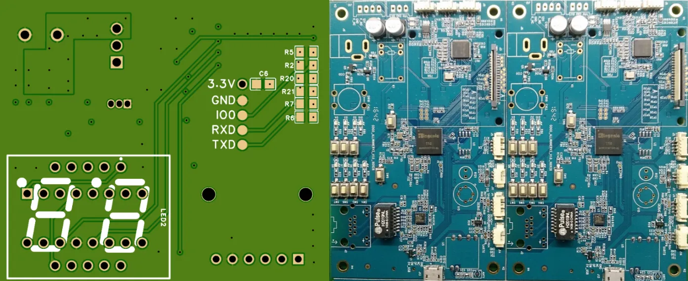
PCB silkscreen is the layer of text and symbols printed on the surface of a circuit board, typically using non-conductive ink. This layer serves as a visual guide, displaying critical information such as component labels, polarity indicators, and assembly instructions. While it doesn’t play a functional role in the board’s electrical performance, silkscreen is invaluable during assembly, testing, and debugging phases.
A poorly designed silkscreen can lead to confusion, misplaced components, and costly rework. On the other hand, a clear and precise silkscreen reduces errors, speeds up assembly, and ensures consistency across production runs. For engineers and assemblers, especially those handling complex designs, silkscreen acts as a roadmap to navigate the intricacies of a PCB.
The Role of Silkscreen in PCB Assembly Efficiency
Silkscreen design directly impacts how quickly and accurately a PCB can be assembled. Whether it’s a small batch assembled by hand or a large-scale automated production, the markings on a board help technicians and machines identify components, orientations, and critical points. Let’s break down the key areas where silkscreen design improves efficiency, focusing on specific aspects like polarity markings, reference designator placement, and aids for manual assembly.
1. Silkscreen Markings for Component Polarity
One of the most common assembly errors is incorrect component orientation, especially for polarized components like diodes, capacitors, and LEDs. A single misplaced component can render a board non-functional or even cause damage during testing. This is where silkscreen markings for component polarity become essential.
By including clear symbols—such as a “+” for positive or a line for the cathode on diodes—silkscreen helps assemblers instantly recognize the correct orientation. For example, on a board with multiple electrolytic capacitors, a small “+” symbol next to the positive pad ensures that each component is placed correctly, even under time pressure. Without these markings, assemblers may need to refer to schematics or datasheets, slowing down the process and increasing the risk of mistakes.
Best Practices for Polarity Markings:
- Use universally recognized symbols (e.g., “+” for positive, “-” for negative).
- Place markings close to the relevant pad or pin, ensuring they are legible even on densely populated boards.
- Avoid overlapping markings with other text or symbols to prevent confusion.
- Ensure the silkscreen ink color contrasts with the board material for visibility (e.g., white ink on a green board).
By following these guidelines, you can reduce assembly errors by as much as 30%, based on industry observations, especially in manual assembly scenarios where human oversight is a factor.
2. Silkscreen Reference Designator Placement
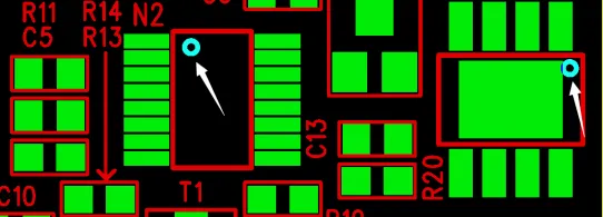
Reference designators are labels like “R1” for resistors, “C3” for capacitors, or “U2” for integrated circuits. These labels correspond to the schematic and help assemblers match components to their correct locations on the board. Proper silkscreen reference designator placement is critical for assembly efficiency, as misplaced or unclear labels can lead to delays and errors.
For instance, if a reference designator is too far from its corresponding component or obscured by other markings, assemblers may struggle to identify the right spot. This issue becomes even more pronounced on high-density boards with hundreds of components. Strategic placement ensures that each label is easily associated with its component, even at a glance.
Guidelines for Effective Reference Designator Placement:
- Position designators as close as possible to the component without overlapping pads or traces.
- Maintain consistent orientation (e.g., all labels aligned horizontally) for readability.
- Use a font size that remains legible after printing—typically 0.8mm or larger, depending on manufacturing capabilities.
- On crowded boards, consider placing designators on both the top and bottom silkscreen layers if components are mounted on both sides.
Implementing these practices can cut down assembly time significantly. For example, a well-organized silkscreen layout can reduce component placement errors by up to 25% in manual assembly, based on feedback from production teams
3. Silkscreen Aids for Manual Assembly
While automation is increasingly common in PCB assembly, manual assembly still plays a vital role, especially for prototypes, small batches, or specialized designs. In these cases, silkscreen aids for manual assembly can make a huge difference in speed and accuracy. These aids include additional markings, instructions, or visual cues that guide technicians through the process.
For example, including arrows to indicate the direction of connector insertion or small notes like “Mount First” near critical components can prevent mistakes during hand assembly. Similarly, outlining test points or labeling specific areas for soldering can help technicians work more confidently without constantly referring to external documentation.
Practical Silkscreen Aids for Manual Assembly:
- Add small directional arrows or symbols near connectors to show insertion orientation.
- Label critical assembly steps directly on the board, such as “Install Jumper Here” for optional configurations.
- Highlight high-risk areas, like heat-sensitive components, with warnings like “Caution: Low Heat.”
- Use dashed lines or boxes to indicate component outlines, making it easier to align parts during placement.
These simple additions can reduce manual assembly time by 15-20%, according to anecdotal reports from small-scale manufacturers, while also lowering the likelihood of errors that require rework.
Additional Benefits of Optimized Silkscreen Design
Beyond the direct impact on assembly, a well-designed silkscreen offers other advantages that contribute to overall project success. These include improved debugging, easier maintenance, and better collaboration between design and assembly teams.
During debugging, for instance, clear silkscreen markings allow technicians to quickly locate specific components or test points without flipping through schematics. This can save hours during fault diagnosis, especially on complex boards with hundreds of components. Similarly, during maintenance or repairs, silkscreen labels help field technicians identify parts and orientations without needing specialized training.
Moreover, a thoughtful silkscreen design fosters better communication between engineers and assemblers. When assembly instructions are embedded directly on the board, there’s less room for misinterpretation, ensuring that the designer’s intent is accurately translated into the final product.
Common Silkscreen Design Mistakes to Avoid
Even with the best intentions, silkscreen design can go wrong if certain pitfalls aren’t addressed. Here are some common mistakes and how to avoid them:
- Overcrowding the Silkscreen: Too much text or too many symbols can make the board look cluttered and confusing. Prioritize essential information and use minimal markings where possible.
- Using Unreadable Fonts: Tiny or overly stylized fonts may look fine on a computer screen but become illegible after printing. Stick to standard, clear fonts with a minimum height of 0.8mm.
- Ignoring Manufacturing Constraints: Not all PCB fabrication processes can handle fine silkscreen details. Check with your manufacturer for minimum line width and spacing requirements—often around 0.15mm for line thickness.
- Placing Markings Over Pads or Vias: Silkscreen ink on solderable areas can interfere with assembly. Ensure markings are offset from pads and other functional elements.
By steering clear of these issues, you can ensure that your silkscreen design enhances rather than hinders the assembly process.
Tips for Collaborating with Manufacturers on Silkscreen Design
Your silkscreen design is only as good as the manufacturing process that brings it to life. Collaborating with your PCB manufacturer early in the design phase can help avoid issues and ensure the best outcome. Here are some tips for effective collaboration:
- Share your silkscreen layer files in a compatible format (e.g., Gerber files) and confirm that all markings are correctly aligned with the board layout.
- Discuss color options for silkscreen ink, as some colors may not provide sufficient contrast on certain board materials. White is often the default for green boards, but yellow or black may work better on lighter surfaces.
- Clarify any specific assembly instructions or markings you want to include, ensuring they meet the manufacturer’s resolution and spacing guidelines.
- Request a prototype or sample board to verify silkscreen legibility before full-scale production.
Taking these steps can prevent costly redesigns and ensure that your silkscreen serves its purpose effectively.
Conclusion: Elevate Your PCB Assembly with Smart Silkscreen Design
Silkscreen design might seem like a minor detail in the grand scheme of PCB production, but its impact on assembly efficiency is undeniable. By focusing on silkscreen markings for component polarity, optimizing silkscreen reference designator placement, and incorporating silkscreen aids for manual assembly, you can streamline workflows, reduce errors, and save valuable time and resources.
Whether you’re working on a prototype or a high-volume production run, investing time in silkscreen optimization pays off in smoother assembly processes and higher-quality results. Start applying these best practices in your next project, and experience the difference a well-designed silkscreen can make.
At ALLPCB, we’re committed to helping you achieve the best possible outcomes for your PCB designs. From design tips to manufacturing support, we’re here to guide you every step of the way. Let’s build better boards together.


