 ALLPCB


In the fast-paced world of electronics, the demand for smaller, faster, and more powerful devices continues to grow. This is where High-Density Interconnect (HDI) PCBs come into play, and at the heart of their production lies a critical process: sequential lamination. But what exactly is sequential lamination, and why is it so important in HDI PCB manufacturing? In short, sequential lamination is a technique used to build multilayer PCBs by adding layers step by step, allowing for the integration of microvias, blind vias, and buried vias to achieve higher circuit density and performance. This blog takes a deep dive into sequential lamination, exploring its role in advanced PCB techniques, the benefits it offers, and how it supports the creation of cutting-edge electronics.
What Is Sequential Lamination in HDI PCB Manufacturing?
Sequential lamination is a manufacturing process used to create multilayer PCBs, especially HDI boards, by bonding layers of materials together in multiple stages. Unlike traditional lamination, where all layers are stacked and bonded in a single step, sequential lamination builds the board layer by layer or in groups of layers. This method allows for greater precision and control, enabling the incorporation of advanced features like microvias, blind vias, and buried vias.
HDI PCBs are designed to pack more functionality into smaller spaces, making them ideal for smartphones, wearables, medical devices, and other compact electronics. Sequential lamination plays a key role in achieving the high circuit density required for these applications by allowing manufacturers to create complex interconnections between layers without sacrificing reliability or performance.
Why Sequential Lamination Matters
In traditional multilayer PCB manufacturing, all layers are laminated at once, and vias (holes that connect layers) are drilled afterward. However, this approach limits the complexity and density of the board. Sequential lamination overcomes these limitations by enabling the creation of vias at different stages of the build process. This results in finer lines, tighter spacing, and more efficient use of space—key characteristics of HDI PCBs.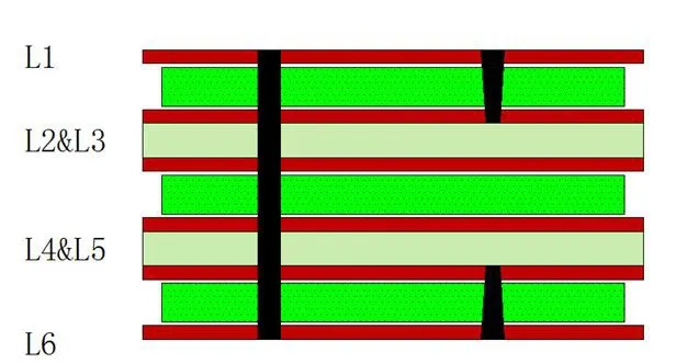 "
"
Key Components of HDI PCBs Enabled by Sequential Lamination
To understand the importance of sequential lamination, it’s essential to look at the specific features it enables in HDI PCBs. These include microvias, blind vias, and buried vias, each of which contributes to the board’s high density and performance.
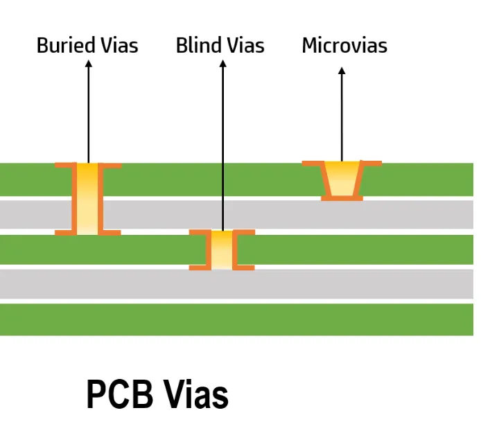
Microvias: The Backbone of High-Density Design
Microvias are tiny holes, typically less than 150 micrometers (6 mils) in diameter, used to connect layers in an HDI PCB. Unlike traditional through-hole vias that span the entire thickness of the board, microvias connect only adjacent layers or a small number of layers. This reduces the space they occupy and allows for denser routing of traces.
Sequential lamination is critical for creating microvias because it allows manufacturers to drill these small holes using laser technology at specific stages of the build. For example, after laminating the first few layers, microvias can be drilled and plated before adding the next set of layers. This precision ensures signal integrity and supports high-speed applications where impedance control is vital, often targeting values as low as 50 ohms for differential pairs.
Blind Vias: Connecting Surface to Inner Layers
Blind vias are another feature made possible by sequential lamination. These vias start on an outer layer of the PCB and connect to an inner layer, but they do not go through the entire board. This design saves space on the opposite side of the board, allowing for more components or routing options.
In sequential lamination, blind vias are created by drilling and plating before the final outer layers are added. This process ensures that the vias are hidden beneath the surface, maintaining a clean layout while maximizing connectivity. Blind vias are especially useful in applications like mobile devices, where every square millimeter of board space counts.
Buried Vias: Hidden Connections for Maximum Density
Buried vias are connections between inner layers of a PCB that are not visible from the surface. These vias are entirely enclosed within the board, making them ideal for high-density designs where surface space is limited. Sequential lamination allows buried vias to be formed by drilling and plating inner layers before they are bonded with additional layers, ensuring they remain hidden and functional.
Buried vias are often used in complex multilayer PCB manufacturing to increase routing density without interfering with surface-mounted components. They are a hallmark of advanced PCB techniques and are frequently found in high-performance electronics like servers and aerospace systems.
How Sequential Lamination Works in Multilayer PCB Manufacturing
The process of sequential lamination involves several carefully controlled steps to ensure the integrity and performance of the final HDI PCB. Below is an overview of how it works:
- Core Layer Preparation: The process begins with a core layer, often made of a thin dielectric material like FR-4 or a high-frequency laminate. Copper traces are etched onto this core to form the initial circuitry.
- First Lamination Cycle: Additional layers of prepreg (a resin-soaked fiberglass material) and copper foil are stacked on top of the core. This stack is then laminated under heat and pressure to bond the materials together.
- Via Formation: After the first lamination, microvias or blind vias are drilled using laser technology. These vias are then plated with copper to establish electrical connections between layers.
- Sequential Build-Up: More layers are added in subsequent lamination cycles, with vias formed as needed at each stage. This build-up can follow structures like 1+n+1 or 2+n+2, where “n” represents the number of core layers, and the numbers on either side indicate the build-up layers on top and bottom.
- Final Lamination and Finishing: Once all layers are added, the board undergoes a final lamination to ensure stability. Surface finishes like ENIG (Electroless Nickel Immersion Gold) are applied to protect the copper and improve solderability.
This step-by-step approach allows for precise control over the placement and quality of vias, ensuring that even complex designs with 8, 10, or more layers can maintain signal integrity at speeds exceeding 10 Gbps in high-speed applications.
Benefits of Sequential Lamination in HDI PCB Production
Sequential lamination offers several advantages that make it indispensable for advanced PCB techniques. Here are some of the key benefits:
- Higher Circuit Density: By enabling the use of microvias, blind vias, and buried vias, sequential lamination allows for more connections in a smaller area, supporting the miniaturization of electronics.
- Improved Signal Integrity: Smaller vias and shorter signal paths reduce parasitic capacitance and inductance, ensuring cleaner signals. This is crucial for high-speed designs where signal delays as small as 100 picoseconds can impact performance.
- Enhanced Design Flexibility: Designers can create complex multilayer structures tailored to specific applications, whether it’s a 6-layer board for a smartphone or a 20-layer board for a data center.
- Reduced Layer Count: By packing more functionality into fewer layers, sequential lamination can lower manufacturing costs and reduce the overall thickness of the PCB.
- Better Thermal Management: With vias strategically placed to dissipate heat, HDI PCBs built with sequential lamination can handle higher power densities without overheating.
Challenges in Sequential Lamination for HDI PCBs
While sequential lamination offers many benefits, it also comes with challenges that manufacturers must address to ensure quality and reliability:
- Complexity and Cost: The multiple lamination cycles and precise drilling required for microvias and other features increase production time and cost compared to traditional methods.
- Material Selection: Choosing the right dielectric materials and prepregs is critical to prevent issues like delamination or warpage during the repeated heating and cooling cycles of lamination.
- Alignment Accuracy: Each layer must be perfectly aligned during lamination to avoid misalignment of vias and traces, which could lead to electrical failures.
- Reliability Concerns: The smaller size of microvias can make them more prone to defects like incomplete plating or cracking under thermal stress, requiring rigorous testing.
Despite these challenges, advancements in manufacturing equipment and quality control processes have made sequential lamination a reliable choice for producing high-performance HDI PCBs.
Applications of HDI PCBs with Sequential Lamination
The unique capabilities of HDI PCBs manufactured with sequential lamination make them suitable for a wide range of industries and applications:
- Consumer Electronics: Smartphones, tablets, and wearables rely on HDI PCBs to fit powerful components into compact designs.
- Medical Devices: Portable diagnostic tools and implantable devices use HDI technology for their small size and high reliability.
- Automotive Systems: Advanced driver-assistance systems (ADAS) and infotainment units benefit from the high-speed signal transmission enabled by HDI boards.
- Aerospace and Defense: Ruggedized electronics in satellites and military equipment use multilayer HDI PCBs for their durability and performance under extreme conditions.
- Telecommunications: High-speed data transfer in 5G infrastructure depends on HDI PCBs to manage complex signal routing with minimal loss.

Future Trends in Sequential Lamination and HDI PCB Manufacturing
As technology continues to evolve, so too will the techniques used in HDI PCB manufacturing. Sequential lamination is likely to play an even bigger role in the future as devices become smaller and more complex. Here are some trends to watch:
- Smaller Microvias: Advances in laser drilling technology will enable even smaller microvias, potentially below 50 micrometers, to support ultra-high-density designs.
- Advanced Materials: New dielectric materials with lower dielectric constants (Dk) and loss tangents (Df) will improve signal performance at frequencies above 20 GHz.
- Automation and Precision: Increased automation in manufacturing will enhance the accuracy of layer alignment and via placement, reducing defects and costs.
- Sustainability: Manufacturers are exploring eco-friendly materials and processes to make sequential lamination more sustainable without compromising quality.
Conclusion: The Power of Sequential Lamination in Advanced PCB Techniques
Sequential lamination is a cornerstone of HDI PCB manufacturing, enabling the creation of compact, high-performance electronics that power our modern world. By facilitating the use of microvias, blind vias, and buried vias, this advanced technique allows for unparalleled circuit density and design flexibility in multilayer PCB manufacturing. While it comes with challenges like increased complexity and cost, the benefits of improved signal integrity, reduced layer count, and enhanced thermal management make it an essential process for industries ranging from consumer electronics to aerospace.
At ALLPCB, we are committed to leveraging cutting-edge technologies like sequential lamination to deliver top-quality HDI PCBs that meet the unique needs of our clients. Whether you’re designing a next-generation smartphone or a critical medical device, understanding the role of sequential lamination can help you make informed decisions about your PCB projects. Stay ahead of the curve by embracing these advanced PCB techniques for your future innovations.


