 ALLPCB


When it comes to manufacturing printed circuit boards (PCBs), selecting the right etching method is crucial for achieving high-quality results. Two popular techniques, plasma etching and chemical etching, often come up in discussions about PCB production. So, which one is better for your project? In short, plasma etching (a dry etching process) offers precision and environmental benefits, making it ideal for intricate designs and advanced applications. On the other hand, chemical etching (a wet etching process) is more cost-effective and widely used for simpler, larger-scale projects, though it may lack the finesse of plasma methods.
In this comprehensive guide, we’ll dive deep into a PCB etching comparison, exploring the differences between these etching methods, including their processes, costs, quality outcomes, and best use cases. Whether you’re weighing etching cost or prioritizing etching quality, this blog will help you make an informed decision for your next PCB project.
What Is PCB Etching and Why Does It Matter?
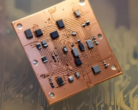
PCB etching is a critical step in the manufacturing process where unwanted copper is removed from a circuit board to create the desired conductive pathways. This process defines the circuitry that allows electronic components to function properly. The choice of etching method directly impacts the precision of these pathways, the overall quality of the board, and the production cost.
Etching can be broadly categorized into two types: wet etching (like chemical etching) and dry etching (like plasma etching). Each method has its own set of advantages and challenges, which we’ll explore in detail. Understanding these differences is essential for engineers and manufacturers aiming to optimize their production process for specific applications, whether it’s for consumer electronics, medical devices, or industrial systems.
Understanding Chemical Etching (Wet Etching)
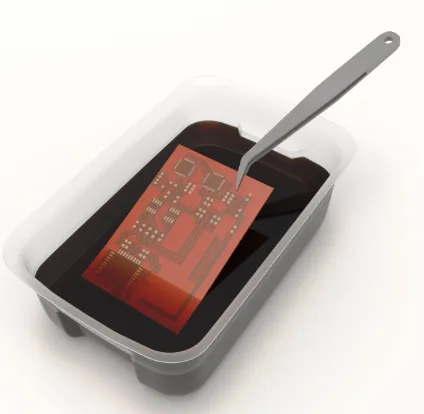
Chemical etching, often referred to as wet etching, is a traditional method used in PCB manufacturing. It involves submerging the PCB in a liquid chemical solution, such as ferric chloride or ammonium persulfate, to dissolve the unprotected copper layers. A protective mask or resist layer is applied to the board to shield the areas that should remain as conductive traces.
How Chemical Etching Works
The process begins by laminating a photoresist layer onto the copper-clad board. A pattern of the desired circuit is then transferred onto the resist using UV light exposure and development. Once the resist is set, the board is immersed in the etching solution. The chemical reacts with the exposed copper, dissolving it while leaving the protected areas intact. After etching, the resist is stripped away, revealing the final circuit pattern.
Advantages of Chemical Etching
- Cost-Effective: Wet etching is generally less expensive than dry methods due to simpler equipment and lower operational costs. For small to medium-scale production, the setup can cost as little as a few hundred dollars for basic systems.
- Scalability: It’s well-suited for high-volume production, as multiple boards can be etched simultaneously in large chemical baths.
- Simplicity: The process is straightforward and doesn’t require advanced technical expertise or complex machinery, making it accessible for many manufacturers.
Challenges of Chemical Etching
- Lower Precision: Chemical etching can result in undercutting, where the etchant eats away at the sides of the copper traces, leading to less defined edges. This can be problematic for fine-pitch designs with trace widths below 0.1 mm.
- Environmental Concerns: The chemicals used are often hazardous, requiring careful handling and disposal. Improper management can lead to environmental pollution.
- Material Waste: The process generates significant chemical waste, which adds to disposal costs and environmental impact.
Understanding Plasma Etching (Dry Etching)
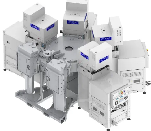
Plasma etching, a form of dry etching, is a more modern and advanced technique that uses ionized gas (plasma) to remove material from the PCB surface. Instead of liquid chemicals, plasma etching relies on a high-energy plasma environment created in a vacuum chamber to etch away unwanted copper or other materials.
How Plasma Etching Works
In plasma etching, the PCB is placed inside a vacuum chamber filled with a reactive gas, such as oxygen or fluorine-based gases. An electric field ionizes the gas, turning it into plasma—a highly reactive state of matter. The plasma bombards the exposed areas of the PCB, physically and chemically removing material with high precision. Similar to chemical etching, a resist layer protects the areas that should remain intact.
Advantages of Plasma Etching
- High Precision: Plasma etching offers superior control, allowing for finer trace widths (down to 0.05 mm or less) and minimal undercutting. This makes it ideal for high-density interconnect (HDI) boards used in advanced electronics.
- Environmental Benefits: Since it doesn’t use liquid chemicals, plasma etching produces less hazardous waste, making it a greener option.
- Versatility: It can etch a variety of materials beyond copper, including dielectrics and polymers, which is useful for multilayer and flexible PCBs.
Challenges of Plasma Etching
- Higher Cost: The equipment for plasma etching is significantly more expensive, often costing tens of thousands of dollars for industrial systems. Operational costs are also higher due to the need for vacuum systems and specialized gases.
- Complexity: The process requires skilled technicians and advanced machinery, which can be a barrier for smaller manufacturers.
- Slower for Bulk Production: Unlike chemical etching, plasma etching often processes boards individually or in smaller batches, which can slow down high-volume production.
Plasma Etching vs. Chemical Etching: A Detailed Comparison
Now that we’ve covered the basics of both methods, let’s compare plasma etching vs. chemical etching across key factors that matter most in PCB manufacturing. This PCB etching comparison will help you decide which method aligns with your project needs.
1. Etching Quality
Chemical Etching: While effective for standard designs, wet etching struggles with ultra-fine features. The isotropic nature of the process (etching equally in all directions) often results in undercutting, reducing the accuracy of trace edges. For designs requiring impedance control, such as high-frequency circuits operating at 5 GHz or above, this can lead to signal integrity issues.
Plasma Etching: Dry etching excels in etching quality due to its anisotropic nature, meaning it etches primarily in one direction (downward). This results in sharper, more precise traces, making it suitable for modern PCBs with tight tolerances, such as those used in 5G technology or microelectronics.
2. Etching Cost
Chemical Etching: Wet etching wins in terms of etching cost. The materials and equipment are relatively affordable, with chemical solutions costing around $10–$20 per gallon for common etchants. For large-scale production, the per-unit cost can drop significantly.
Plasma Etching: Dry etching is more expensive due to the high initial investment in equipment and ongoing costs for gases and maintenance. A single plasma etching system can cost upwards of $50,000, making it less viable for budget-conscious projects or low-volume runs.
3. Speed and Scalability
Chemical Etching: Wet etching is faster for bulk production since multiple boards can be processed in a single chemical bath. A typical cycle might take 10–30 minutes per batch, depending on the copper thickness (e.g., 1 oz or 2 oz per square foot).
Plasma Etching: Dry etching is generally slower, as it often processes boards one at a time or in small batches within a vacuum chamber. Etching a single board might take 5–15 minutes, which can add up in high-volume scenarios.
4. Environmental Impact
Chemical Etching: The use of harsh chemicals poses environmental risks. Disposal of spent etchant solutions must comply with strict regulations, adding to operational costs. For instance, improper disposal can result in fines or penalties in many regions.
Plasma Etching: Dry etching is more environmentally friendly, producing minimal waste. The gases used can often be neutralized or recycled within the system, reducing the ecological footprint.
Choosing the Right Etching Method for Your PCB Project
Deciding between dry etching and wet etching depends on your project’s specific requirements. Here are some guidelines to help you choose:
- Opt for Chemical Etching If: You’re working on a budget, producing standard PCBs with larger trace widths (above 0.2 mm), or need to scale up production quickly. It’s ideal for simpler designs used in consumer electronics like basic power supplies or LED circuits.
- Opt for Plasma Etching If: Your project demands high precision for fine-pitch components, involves HDI boards, or requires environmentally friendly processes. It’s perfect for advanced applications like telecommunications equipment or medical devices with strict signal integrity needs (e.g., maintaining impedance at 50 ohms for RF signals).
Future Trends in PCB Etching Methods
As technology advances, both etching methods are evolving. Chemical etching processes are becoming more sustainable with the development of recyclable etchants and closed-loop systems that minimize waste. Meanwhile, plasma etching is gaining traction in industries requiring nanoscale precision, such as semiconductor manufacturing, where features as small as 10 nm are becoming common.
Hybrid approaches, combining elements of both wet and dry etching, are also emerging. These methods aim to balance cost and precision, catering to a wider range of PCB applications. Staying informed about these trends can help manufacturers remain competitive in a rapidly changing field.
Conclusion
Choosing between plasma etching vs. chemical etching for PCB manufacturing boils down to your project’s priorities. If cost and scalability are your main concerns, chemical etching offers a reliable and affordable solution for standard designs. However, if precision and environmental impact are critical—especially for cutting-edge applications—plasma etching is the superior choice despite its higher etching cost.
By understanding the strengths and limitations of each method through this PCB etching comparison, you can make a decision that aligns with your technical and budgetary needs. Whether you prioritize etching quality or efficiency, selecting the right process ensures your PCBs meet the demands of today’s fast-paced electronics industry.


