ALLPCB


Are you looking to understand the electrolytic gold plating process for PCB gold fingers? This guide dives deep into the step-by-step method of applying gold plating on nickel for durable and reliable edge connectors. From preparing the PCB to controlling plating thickness, using a chemical bath for gold plating, and mastering PCB gold finger electroplating, we’ve got you covered with practical insights and detailed explanations. Let’s explore how this critical process ensures high conductivity and corrosion resistance for your printed circuit boards.
Introduction to PCB Gold Fingers and Their Importance
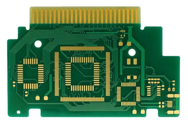
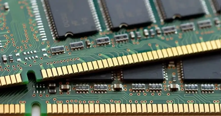
Gold fingers, also known as edge connectors, are the gold-plated pads found on the edges of printed circuit boards (PCBs). These components are essential for creating reliable electrical connections between the PCB and other devices, such as in computer memory modules, graphics cards, and industrial equipment. The gold plating on these fingers provides excellent conductivity, resistance to corrosion, and durability against repeated insertions and removals.
The electrolytic gold plating process is a widely used method to apply this gold layer over a nickel base. Unlike other surface finishes, gold plating ensures long-term performance in harsh environments. In this blog, we’ll walk you through the detailed steps of PCB gold finger electroplating, focusing on nickel plating for gold fingers, controlling plating thickness, and the chemical baths involved.
Why Use Electrolytic Gold Plating for PCB Gold Fingers?
Electrolytic gold plating, also known as hard gold plating, is preferred for PCB gold fingers due to its durability and wear resistance. This process involves depositing a layer of gold over a nickel undercoat using an electric current. The result is a robust coating that can withstand up to 1,000 insertion cycles without significant wear, making it ideal for applications requiring frequent connections.
Gold plating on nickel also prevents oxidation, ensuring a stable electrical connection with low contact resistance, often below 10 milliohms. Additionally, the nickel layer acts as a barrier, preventing copper diffusion from the PCB substrate into the gold, which could otherwise degrade performance over time.
Step-by-Step Guide to the Electrolytic Gold Plating Process
Let’s break down the electrolytic gold plating process for PCB gold fingers into clear, actionable steps. This method ensures precision and consistency, which are critical for high-quality edge connectors.
Step 1: Surface Preparation and Cleaning
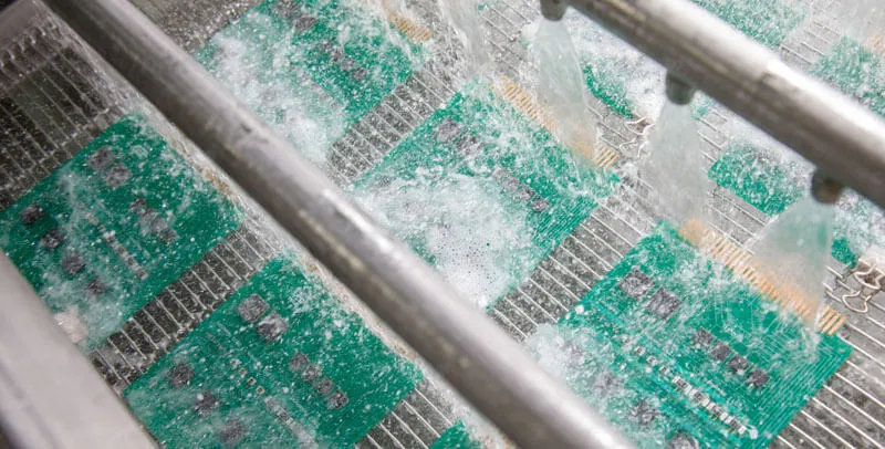
The first step in PCB gold finger electroplating is preparing the board’s surface. Any contaminants like oils, dust, or oxides on the copper pads can interfere with adhesion during plating. The PCB undergoes a thorough cleaning process using alkaline solutions or micro-etching to remove impurities and create a uniform surface.
This step is crucial because even minor residues can lead to uneven plating or poor bonding between the nickel and gold layers. After cleaning, the board is rinsed with deionized water to eliminate any remaining chemicals.
Step 2: Nickel Plating for Gold Fingers
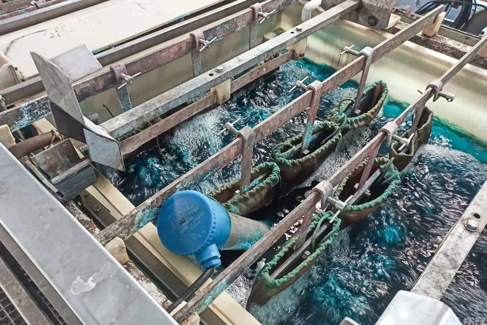
Before applying gold, a layer of nickel is plated onto the copper pads of the gold fingers. Nickel plating for gold fingers serves as a barrier layer, preventing the copper from migrating into the gold coating, which could cause corrosion or reduced conductivity over time. This step typically uses an electrolytic nickel bath, where the PCB is immersed in a solution containing nickel salts, and an electric current deposits a uniform nickel layer.
The thickness of the nickel layer is usually between 100 and 200 microinches (2.5 to 5 micrometers), depending on the application’s requirements. Controlling the thickness at this stage is vital to ensure a stable foundation for the gold layer.
Step 3: Activation for Gold Adhesion
After nickel plating, the surface is activated to improve gold adhesion. This often involves a mild acid rinse or a specialized activation solution that prepares the nickel surface for the gold plating process. Activation ensures that the gold bonds effectively to the nickel, avoiding issues like peeling or flaking during use.
Step 4: Gold Plating on Nickel Using Electrolytic Process
Now comes the core of the process: gold plating on nickel. The PCB is immersed in a chemical bath for gold plating, which contains a gold electrolyte solution, typically gold cyanide or gold sulfite. During PCB gold finger electroplating, an electric current is applied, with the PCB acting as the cathode (negative electrode) and a gold anode (positive electrode) supplying the gold ions.
The electric current drives the gold ions to deposit onto the nickel-coated gold fingers. The result is a hard gold layer, often alloyed with small amounts of cobalt or nickel (about 0.1-0.3%) to enhance durability. This hard gold coating typically ranges from 30 to 50 microinches (0.76 to 1.27 micrometers) thick for most applications, ensuring both conductivity and wear resistance.
Step 5: Controlling Plating Thickness for Consistency
Controlling plating thickness is a critical aspect of the electrolytic gold plating process. Too thin a layer may not provide adequate protection or conductivity, while too thick a layer can increase costs unnecessarily. Manufacturers use precise current control and timing to achieve the desired thickness. For instance, a current density of 5-10 amperes per square foot is often used to deposit gold at a controlled rate.
Advanced systems may also employ X-ray fluorescence (XRF) testing to measure the thickness of both nickel and gold layers non-destructively. This ensures compliance with industry standards, such as IPC-6012, which specifies minimum gold thickness for different classes of PCBs (e.g., 30 microinches for Class 2 boards).
Step 6: Rinsing and Drying
After gold plating, the PCB is rinsed again with deionized water to remove any residual electrolyte solution from the chemical bath for gold plating. This prevents contamination or corrosion on the board. The PCB is then dried using compressed air or a low-temperature oven to avoid thermal stress on the components.
Step 7: Final Inspection and Quality Control
The final step involves a thorough inspection of the gold fingers. Manufacturers check for uniform thickness, adhesion quality, and the absence of defects like pitting or discoloration. Electrical testing may also be conducted to verify low contact resistance, often targeting values below 10 milliohms for reliable connections.
Key Factors in the Electrolytic Gold Plating Process
Several factors influence the success of PCB gold finger electroplating. Understanding these can help ensure consistent results and high-quality edge connectors.
Chemical Bath Composition
The chemical bath for gold plating must be carefully formulated and maintained. The concentration of gold ions, pH level (typically between 4.0 and 4.5), and temperature (around 50-60°C) all affect the deposition rate and quality of the gold layer. Regular monitoring and replenishment of the bath are necessary to avoid defects like uneven plating or porosity.
Current Density and Distribution
Uniform current distribution across the PCB is essential for even plating. Areas with higher current density may receive thicker deposits, leading to inconsistencies. Using auxiliary anodes or shielding can help balance the current and achieve uniform thickness on all gold fingers.
Material Compatibility
The choice of materials for both the nickel and gold layers must be compatible with the PCB’s base materials and intended application. For instance, hard gold with cobalt additives is often used for high-wear applications, while softer gold may be suitable for less demanding environments.
Benefits of Electrolytic Gold Plating for PCB Gold Fingers
The electrolytic gold plating process offers several advantages that make it the go-to choice for PCB gold fingers:
- High Durability: Hard gold withstands thousands of insertion cycles without significant wear.
- Corrosion Resistance: Gold does not oxidize, ensuring long-term reliability in humid or corrosive environments.
- Low Contact Resistance: Provides stable electrical connections with resistance values often below 10 milliohms.
- Precision Control: Allows for accurate control over thickness and uniformity, meeting strict industry standards.
Common Challenges and How to Overcome Them
While the electrolytic gold plating process is highly effective, it’s not without challenges. Here are some common issues and solutions:
Uneven Plating Thickness
Uneven current distribution can cause variations in gold thickness. Using proper fixturing and optimizing bath agitation can help ensure uniform deposition.
Poor Adhesion
Inadequate surface preparation or contamination can lead to poor adhesion between layers. Strict cleaning protocols and activation steps can mitigate this risk.
High Costs
Gold plating can be expensive due to material costs. Selective plating, where gold is applied only to the gold fingers, can reduce expenses without compromising performance.
Conclusion: Mastering PCB Gold Finger Plating
The electrolytic gold plating process is a cornerstone of creating reliable and durable PCB gold fingers. By following the detailed steps—from surface preparation and nickel plating for gold fingers to controlling plating thickness and using the right chemical bath for gold plating—you can achieve high-quality edge connectors that meet the demands of modern electronics.
Understanding the nuances of PCB gold finger electroplating, such as current density, bath composition, and quality control, ensures that your boards deliver exceptional conductivity and longevity. Whether you’re designing for consumer electronics or industrial applications, mastering gold plating on nickel will elevate the performance of your PCBs.