 ALLPCB


Gold finger beveling is a critical process in PCB manufacturing that ensures smooth insertion and reduces wear and tear on connectors. But why does it matter, and how can you ensure it’s done correctly? In this comprehensive guide, we’ll dive deep into the importance of the PCB gold finger bevel angle, the gold finger beveling process, and the role of beveling for smooth insertion and beveling to reduce wear and tear. We’ll also explore the benefits of using automated beveling machines for precision and efficiency. Whether you’re an engineer or a manufacturer, this blog will provide actionable insights to optimize your PCB designs.
What Are PCB Gold Fingers and Why Do They Need Beveling?
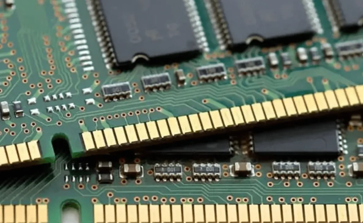
Gold fingers, also known as edge connectors, are the gold-plated pads or contacts located along the edge of a printed circuit board (PCB). These connectors are designed to interface with slots or sockets in devices like computers, graphics cards, or industrial equipment. The gold plating offers excellent conductivity, corrosion resistance, and durability, making it ideal for repeated insertions and removals.
However, without proper finishing, the sharp edges of gold fingers can cause issues. This is where beveling comes in. Beveling is the process of cutting or grinding the edge of the gold finger at a specific angle, typically between 30 and 45 degrees, to create a smoother transition. This angled edge reduces friction during insertion, minimizes damage to the connector and socket, and extends the lifespan of the PCB.
The Importance of PCB Gold Finger Beveling
Beveling isn’t just a cosmetic step; it plays a vital role in the functionality and reliability of a PCB. Let’s break down why beveling for smooth insertion and beveling to reduce wear and tear are essential:
- Improved Insertion: A properly beveled edge allows the PCB to slide into a socket with minimal resistance. Without beveling, sharp edges can catch on the socket, making insertion difficult and potentially damaging both the PCB and the slot.
- Reduced Wear and Tear: Repeated insertions can wear down both the gold plating on the fingers and the contacts in the socket. A beveled edge distributes contact pressure more evenly, reducing mechanical stress and extending the lifespan of the connection. Studies suggest that properly beveled edges can increase connector durability by up to 20% over non-beveled edges.
- Enhanced Signal Integrity: Sharp edges or damaged connectors can lead to poor contact, resulting in signal loss or interference. Beveling helps maintain consistent contact, ensuring reliable signal transmission, especially in high-speed applications where impedance control is critical (e.g., maintaining 50 ohms for high-frequency signals).
- Prevention of Debris: Beveling minimizes the risk of scraping off material from the socket or PCB during insertion, which can create debris and lead to connection issues over time.
Understanding the PCB Gold Finger Bevel Angle
The PCB gold finger bevel angle is a crucial factor in achieving optimal performance. The angle at which the edge is cut directly impacts how smoothly the PCB inserts into a socket and how much wear it experiences over time.
Common bevel angles range from 30 to 45 degrees, with 30 degrees being the most widely used for standard applications. A 30-degree angle provides a balance between ease of insertion and maintaining sufficient contact area for conductivity. For more specialized applications, such as high-density connectors, a 45-degree angle might be preferred to further reduce insertion force.
Choosing the right angle depends on several factors, including the type of socket, the frequency of insertion, and the specific design requirements of the PCB. For instance, in high-speed data transfer applications (e.g., PCIe cards operating at 8 GT/s or higher), a slightly steeper angle might be used to minimize signal degradation caused by uneven contact.
The Gold Finger Beveling Process: Step by Step
The gold finger beveling process requires precision and attention to detail to ensure consistent results. Here’s a step-by-step overview of how it’s done:
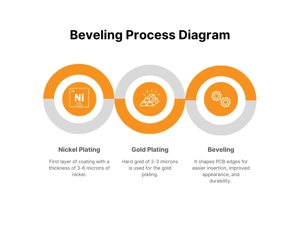
- Design and Planning: Before manufacturing begins, engineers specify the bevel angle and dimensions in the PCB design files. This ensures the beveling process aligns with the intended application and socket requirements.
- Gold Plating: The edge connectors are plated with a layer of hard gold, typically 30 to 50 microinches thick, to provide conductivity and durability. The plating must be uniform to prevent uneven wear during beveling.
- Beveling: Using specialized equipment, the edges of the gold fingers are cut or ground at the predetermined angle. This step can be done manually for small batches, but automated beveling machines are often used for high-volume production to ensure consistency and speed.
- Inspection: After beveling, the edges are inspected for smoothness and accuracy. Any burrs or irregularities are removed to prevent issues during insertion. Advanced manufacturers use optical inspection systems to verify the bevel angle and surface quality.
- Final Testing: The PCB undergoes functional testing to confirm that the beveled gold fingers make proper contact with the socket and maintain signal integrity under operating conditions.
Beveling for Smooth Insertion and Reduced Wear: Best Practices
Achieving beveling for smooth insertion and beveling to reduce wear and tear requires adherence to best practices during design and manufacturing. Here are some actionable tips for engineers and manufacturers:
- Specify the Correct Bevel Angle: Work closely with your manufacturing partner to determine the ideal bevel angle based on the PCB’s application. For high-frequency or high-insertion applications, consider testing multiple angles to find the best fit.
- Use High-Quality Materials: Ensure the gold plating meets industry standards (e.g., MIL-G-45204 for hard gold) to withstand repeated insertions without degrading. Poor-quality plating can lead to uneven beveling and faster wear.
- Maintain Tight Tolerances: The beveling process must be precise to avoid variations in angle or edge smoothness. Even a deviation of 1-2 degrees can impact insertion force and contact reliability.
- Test Under Real Conditions: Simulate the insertion and removal process during the design phase to identify potential issues. For example, test the PCB with the target socket for at least 500 cycles to assess wear patterns.
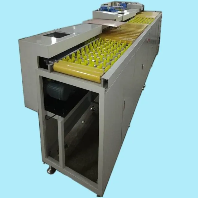
The Role of Automated Beveling Machines in Precision Manufacturing
In modern PCB production, automated beveling machines have become indispensable for achieving consistent, high-quality results. These machines offer several advantages over manual beveling, especially for large-scale manufacturing:
- Consistency: Automated machines can maintain the same bevel angle and edge smoothness across thousands of PCBs, reducing variability and ensuring every board meets specifications.
- Speed: Manual beveling is time-consuming, especially for complex designs with multiple edge connectors. Automated systems can process boards at a much faster rate, improving production efficiency.
- Precision: Advanced beveling machines use computer-controlled cutting tools and optical sensors to achieve tolerances as tight as ±0.1 degrees. This level of accuracy is critical for high-reliability applications.
- Cost-Effectiveness: While the initial investment in automated equipment is higher, the reduction in labor costs and rework makes it a cost-effective solution for high-volume runs.
For example, in a production run of 10,000 PCBs for a server application, using an automated beveling machine can reduce processing time by up to 40% compared to manual methods, while also minimizing defects related to inconsistent beveling.
Common Challenges in Gold Finger Beveling and How to Overcome Them
Despite its importance, the beveling process can present challenges that impact the quality of the final product. Here are some common issues and solutions:
- Uneven Beveling: This can occur due to worn-out cutting tools or improper machine calibration. Regular maintenance of beveling equipment and using high-quality tools can prevent this issue.
- Gold Plating Damage: Excessive pressure during beveling can strip or damage the gold layer. Adjusting the machine settings to apply gentle, consistent pressure helps protect the plating.
- Burrs or Rough Edges: Burrs can form if the cutting tool is dull or the bevel angle is too steep. Implementing a secondary polishing step or using finer cutting tools can smooth out the edges.
- Inconsistent Angles: Variations in bevel angle across a batch can lead to insertion issues. Automated machines with real-time monitoring systems can detect and correct deviations during production.
How to Choose the Right Manufacturing Partner for Gold Finger Beveling
Selecting a reliable manufacturing partner is key to achieving high-quality gold finger beveling. Here are some factors to consider:
- Experience: Look for a manufacturer with a proven track record in producing PCBs with gold fingers for applications similar to yours.
- Equipment: Ensure the manufacturer uses modern automated beveling machines and inspection tools to guarantee precision and consistency.
- Quality Control: A robust quality assurance process, including visual and functional testing, is essential to catch defects early.
- Customization: Your partner should be able to tailor the bevel angle and process to meet your specific design requirements.
Conclusion: Perfecting PCB Gold Finger Beveling for Long-Term Reliability
Gold finger beveling is a small but critical step in PCB manufacturing that directly impacts the performance and durability of edge connectors. By focusing on the right PCB gold finger bevel angle, following a precise gold finger beveling process, and leveraging automated beveling machines, manufacturers can achieve beveling for smooth insertion and beveling to reduce wear and tear. These efforts result in reliable, long-lasting connections that meet the demands of modern electronics.
Whether you’re designing a high-speed data card or a rugged industrial controller, paying attention to beveling can make all the difference. Partner with a trusted manufacturer to ensure your PCBs are built to the highest standards, delivering consistent performance in every application.


