ALLPCB


Pad lifting is a common issue in printed circuit board (PCB) manufacturing that can compromise the reliability and functionality of electronic devices. If you're searching for ways to prevent PCB pad lifting, you're in the right place. This blog post offers a proactive approach to tackling pad lifting through effective design, assembly techniques, and material selection. By implementing the strategies discussed here, such as optimizing PCB design, refining SMT assembly processes, and choosing the right materials, you can significantly reduce the risk of pad lifting and ensure long-term PCB reliability.
In the sections below, we'll dive deep into the causes of pad lifting and provide actionable solutions for preventing issues during PCB design, SMT assembly, wave soldering, and material selection. Whether you're an engineer, designer, or manufacturer, this guide will equip you with practical knowledge to enhance the durability of your boards.
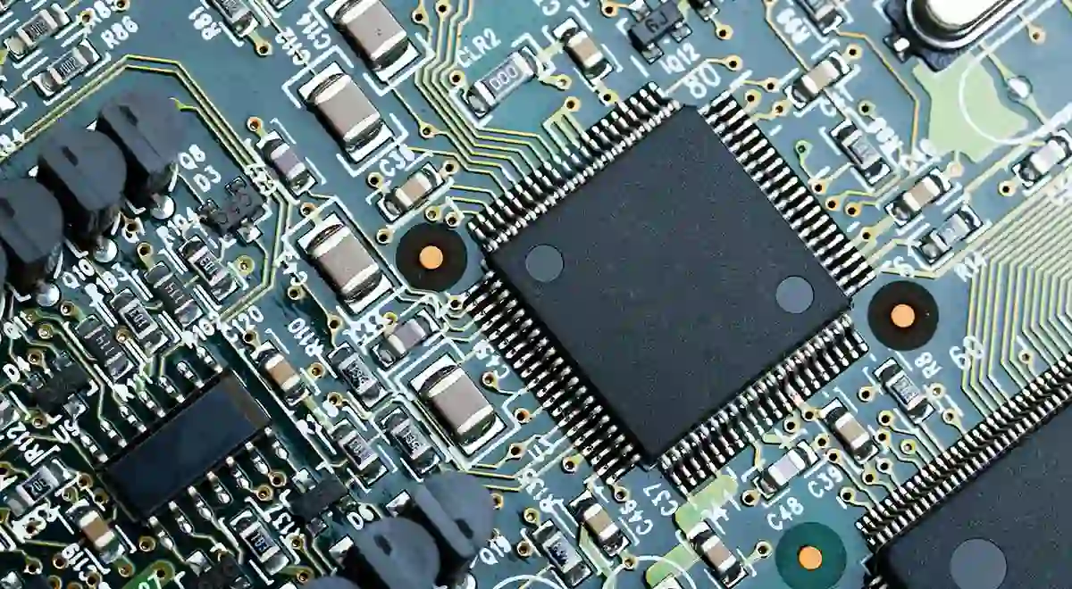
What Is Pad Lifting and Why Does It Matter?
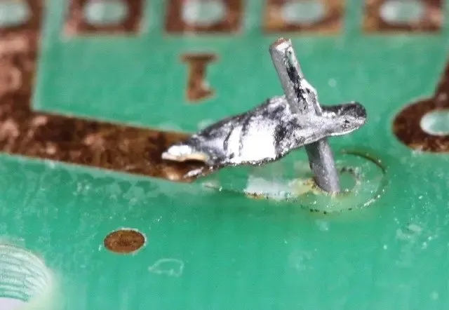
Pad lifting occurs when a copper pad on a PCB detaches from the board's surface, disrupting the connection between components and the copper traces. This issue often leads to electrical failures, reduced performance, or complete device malfunction. Pad lifting is particularly common in single-layer boards but can affect multilayer designs as well, especially under thermal or mechanical stress.
The impact of pad lifting is significant. A single lifted pad can cause a component to fail, leading to costly repairs or product recalls. For industries like automotive, aerospace, and medical devices, where reliability is critical, preventing pad lifting is a top priority. Understanding the root causes—such as poor adhesion, excessive heat during soldering, or improper handling—is the first step toward prevention.
Common Causes of PCB Pad Lifting
Before diving into prevention strategies, let's explore the primary reasons why pad lifting happens. Identifying these causes helps in targeting specific areas for improvement.
- Thermal Stress: Excessive heat during soldering processes, like SMT assembly or wave soldering, can weaken the bond between the pad and the PCB substrate, causing delamination.
- Mechanical Stress: Physical handling, component insertion, or rework can apply undue force on pads, leading to lifting.
- Poor Material Selection: Low-quality substrates or laminates with weak adhesion properties increase the risk of pad detachment.
- Design Flaws: Inadequate pad size, improper trace routing, or insufficient solder mask coverage can contribute to pad lifting during manufacturing or use.
- Moisture Absorption: PCBs exposed to humid environments can absorb moisture, which expands during soldering and causes pads to lift.
By addressing these root causes, you can take proactive steps to prevent PCB pad lifting and improve overall board reliability.
Prevent PCB Pad Lifting with Effective Design Strategies
One of the most effective ways to prevent PCB pad lifting is to focus on robust design practices. A well-thought-out design minimizes stress on pads and ensures strong adhesion to the substrate. Here are key strategies for tackling PCB design pad lifting:
Optimize Pad Size and Shape
Designing pads that are appropriately sized for the components they support is crucial. Pads that are too small may not provide enough surface area for soldering, leading to weak joints and potential lifting. Conversely, oversized pads can cause uneven heat distribution during soldering, increasing thermal stress. As a general rule, follow the component manufacturer's recommended pad dimensions, often found in datasheets. For example, a standard 0603 SMD resistor typically requires a pad size of 0.9mm x 0.8mm with a 0.6mm gap between pads.
Use Teardrop Pads for Added Strength
Teardrop-shaped pads, where the pad extends slightly into the trace, can reinforce the connection and reduce the risk of lifting. This design helps distribute mechanical stress more evenly, especially in high-stress areas like connectors or through-hole components.
Implement Proper Solder Mask Coverage
Ensure that the solder mask extends slightly over the edges of the pad to anchor it to the board. However, avoid excessive overlap, as it can trap moisture or contaminants that weaken adhesion. A typical solder mask clearance of 0.1mm to 0.2mm around the pad is often ideal for most designs.
SMT Assembly Pad Lifting: Best Practices for Prevention
Surface Mount Technology (SMT) assembly involves precise soldering of components onto PCB pads, often under high temperatures. Improper SMT processes can easily lead to pad lifting. Here are actionable tips to prevent SMT assembly pad lifting:
Control Reflow Soldering Temperatures
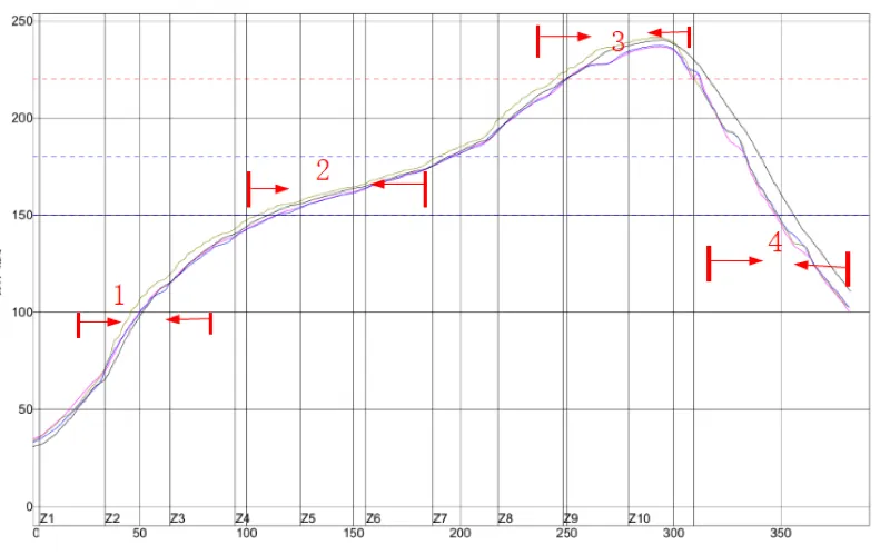
During reflow soldering, excessive heat or rapid temperature changes can cause thermal shock, weakening pad adhesion. Stick to the recommended reflow profile for your solder paste, typically involving a preheat stage (150-180°C for 60-90 seconds), a soak stage, and a peak temperature of around 240-260°C for lead-free solder. Use a thermal profiler to monitor and adjust temperatures in real-time.
Use Adequate Solder Paste Volume
Applying too little solder paste can result in weak joints, while too much can cause bridging or uneven heating, both of which increase the risk of pad lifting. Ensure stencil apertures are designed to deposit a consistent layer of paste, typically 0.1mm to 0.15mm thick, depending on the component size.
Minimize Rework
Reworking soldered components often involves additional heat cycles, which can stress pads and lead to lifting. Train assembly teams to follow precise soldering techniques and use tools like hot air rework stations with controlled temperatures (below 300°C) to avoid overheating.
Wave Soldering Pad Lifting: Tips for a Reliable Process
Wave soldering, commonly used for through-hole components, exposes PCBs to molten solder waves at high temperatures, posing a risk of pad lifting if not managed properly. Here’s how to prevent wave soldering pad lifting:
Adjust Wave Soldering Parameters
Maintain solder bath temperatures between 250-270°C for lead-free solder, and ensure the conveyor speed allows for a contact time of 2-4 seconds with the solder wave. Prolonged exposure can overheat the board, causing pad delamination. Regularly calibrate equipment to avoid temperature spikes.
Pre-Bake PCBs to Remove Moisture
Moisture trapped in the PCB substrate can expand during wave soldering, leading to pad lifting. Pre-baking boards at 100-120°C for 2-4 hours before soldering can eliminate absorbed moisture, especially for boards stored in humid environments.
Secure Components Before Soldering
Ensure components are firmly secured to the board using adhesives or fixtures before wave soldering. Loose components can create mechanical stress on pads during the process, increasing the likelihood of lifting.
Material Selection Pad Lifting: Choosing the Right Components
The materials used in PCB fabrication play a critical role in pad adhesion and overall board reliability. Poor material choices can lead to weak bonds and increased susceptibility to lifting. Here are key considerations for material selection pad lifting prevention:
Select High-Quality Substrates
Choose substrates with strong adhesion properties, such as FR-4 with a high glass transition temperature (Tg) of 150°C or above. Higher Tg materials resist thermal deformation during soldering, reducing the risk of pad lifting. For high-frequency or high-temperature applications, consider materials like polyimide, though they are more expensive.
Use Reliable Copper Foil
The copper foil used for pads and traces should have a roughened surface to enhance bonding with the substrate. Electrodeposited (ED) copper with a thickness of 1 oz/ft2 (35 μm) is a common choice for standard applications, providing a good balance of adhesion and conductivity.
Opt for Moisture-Resistant Finishes
Surface finishes like ENIG (Electroless Nickel Immersion Gold) or HASL (Hot Air Solder Leveling) can protect pads from oxidation and moisture absorption, both of which weaken adhesion over time. ENIG, for instance, offers a flat surface and excellent corrosion resistance, making it ideal for fine-pitch components.
Additional Proactive Measures for PCB Reliability
Beyond design, assembly, and material selection, there are broader practices that contribute to preventing pad lifting and enhancing overall PCB reliability:
Implement Rigorous Quality Control
Conduct thorough inspections at every stage of PCB production, from fabrication to assembly. Use automated optical inspection (AOI) systems to detect early signs of pad lifting or weak solder joints. Testing boards under thermal and mechanical stress can also identify potential weaknesses before they become failures.
Train Staff on Proper Handling
Improper handling during assembly or rework can cause mechanical stress on pads. Train staff to use anti-static tools, avoid excessive force when placing components, and follow standardized procedures for soldering and rework.
Store PCBs in Controlled Environments
Store bare PCBs and assembled boards in low-humidity environments (below 50% relative humidity) to prevent moisture absorption. Use vacuum-sealed bags with desiccants for long-term storage, especially in tropical or humid regions.
Conclusion: Building Reliable PCBs with Pad Lifting Prevention
Pad lifting is a preventable issue that, if addressed proactively, can significantly improve the reliability and performance of your PCBs. By focusing on robust PCB design practices to prevent PCB design pad lifting, optimizing SMT assembly and wave soldering processes to avoid SMT assembly pad lifting and wave soldering pad lifting, and making informed choices in material selection to tackle material selection pad lifting, you can minimize risks and ensure durable connections.
At every stage of PCB production, from design to final assembly, attention to detail is key. Implementing the strategies outlined in this guide—such as controlling soldering temperatures, using high-quality materials, and enforcing strict quality control—will help you create boards that stand the test of time. With a proactive approach to prevent PCB pad lifting, you’re not just solving a problem; you’re building trust in the reliability of your electronic products.