 ALLPCB


If you're looking to streamline your PCB manufacturing process, optimizing your design for flying probe testing is a game-changer. This testing method ensures your printed circuit boards (PCBs) are free from electrical faults before they reach the market. But how do you design for flying probe testing to ensure accessibility and accuracy? In this comprehensive guide, we'll dive into practical tips and tricks for design for flying probe testing, focusing on flying probe testing test point placement, flying probe testing accessibility, and essential flying probe testing rules to follow. Whether you're a seasoned engineer or new to PCB design, this post will help you create boards that are easier and faster to test.
What is Flying Probe Testing and Why Does It Matter?
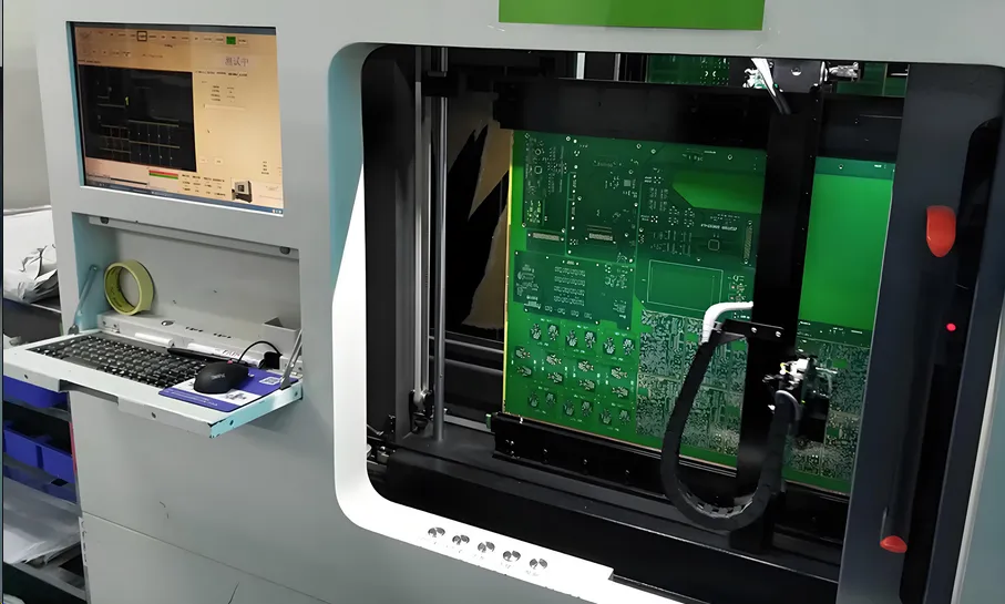
Flying probe testing is a method used in PCB manufacturing to check for electrical issues like shorts, opens, and incorrect component values without the need for a custom test fixture. Unlike traditional in-circuit testing (ICT), which requires a dedicated test jig, flying probe testing uses movable probes that "fly" across the board to contact specific test points. This makes it ideal for low to mid-volume production runs, prototypes, or boards with accessibility challenges.
The benefits are clear: reduced setup costs, faster testing for small batches, and flexibility for complex designs. However, to take full advantage of this method, your PCB design must be optimized for probe access and accuracy. Poor design choices can lead to missed faults, longer testing times, or even damage to the board. Let's explore how to avoid these pitfalls with actionable strategies tailored for design for flying probe testing.
Key Principles of Design for Flying Probe Testing
Designing a PCB with flying probe testing in mind starts with understanding the limitations and requirements of the testing equipment. The probes need clear access to test points, and the layout must minimize the risk of errors during testing. Below are the core principles to follow for effective design for flying probe testing.
1. Prioritize Accessibility for Probes
One of the most critical aspects of flying probe testing accessibility is ensuring that the probes can physically reach the test points on your PCB. Flying probe machines typically have probes with a minimum diameter of around 0.1 mm to 0.2 mm, and they need a clear path to make contact without interference from components or other board features.
- Spacing: Maintain a minimum clearance of 0.5 mm between test points and nearby components or traces to prevent probe misalignment or accidental contact with adjacent elements.
- Component Height: Avoid placing tall components (above 6 mm) near test points, as they can block probe access. If unavoidable, ensure the probe can approach from an angle or adjust the test point location.
- Edge Clearance: Keep test points at least 3 mm away from the PCB edges to avoid probe overtravel risks during testing.
By focusing on these spacing and clearance rules, you ensure that the probes can navigate your board without issues, reducing test setup time and potential errors.
2. Strategic Flying Probe Testing Test Point Placement
The placement of test points is a cornerstone of effective flying probe testing test point placement. Test points are specific pads or vias on the PCB where probes make contact to measure electrical properties. Poor placement can lead to inaccurate readings or prolonged testing times. Here are some best practices:
- Uniform Distribution: Distribute test points evenly across the board to minimize probe travel time. For a typical 100 mm x 100 mm board, aim for at least one test point per 25 mm2 area for comprehensive coverage.
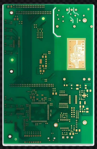
- Size Matters: Ensure test points are large enough for reliable contact. A diameter of 0.8 mm to 1.2 mm is generally recommended for most flying probe systems.
- Net Coverage: Place test points on every critical net, especially power, ground, and high-speed signal lines (e.g., signals operating above 100 MHz), to verify connectivity and integrity.
- Avoid Congested Areas: Don’t place test points under components or in densely populated areas where probes can’t reach. If necessary, use vias as test points on the opposite side of the board.
Proper test point placement not only speeds up the testing process but also ensures that no critical area of the PCB is left untested.
3. Adhere to Flying Probe Testing Rules
Following established flying probe testing rules is essential to avoid common design mistakes that could hinder the testing process. These rules are often based on industry standards and equipment capabilities. Here are some key guidelines:
- Double-Sided Access: If your PCB is double-sided, ensure test points are accessible on both sides. Most flying probe systems can test both sides, but you must specify this in your design files and avoid blocking access with components.
- Probe Angle Limitations: Flying probes typically operate at angles between 0° and 10° from vertical. Design your test points to accommodate this limited range, avoiding deep cavities or recessed areas.
- Material Considerations: Ensure that test points are free from solder mask or other coatings that could insulate them. Bare copper or gold-plated pads are ideal for consistent probe contact.
By sticking to these rules, you create a PCB layout that aligns with the capabilities of flying probe testing equipment, ensuring accurate results without delays.
Tips and Tricks for Optimizing Your PCB Design
Beyond the basic principles, there are several advanced tips and tricks that can further enhance your PCB design for flying probe testing. These strategies focus on efficiency, error prevention, and collaboration with your manufacturing partner.
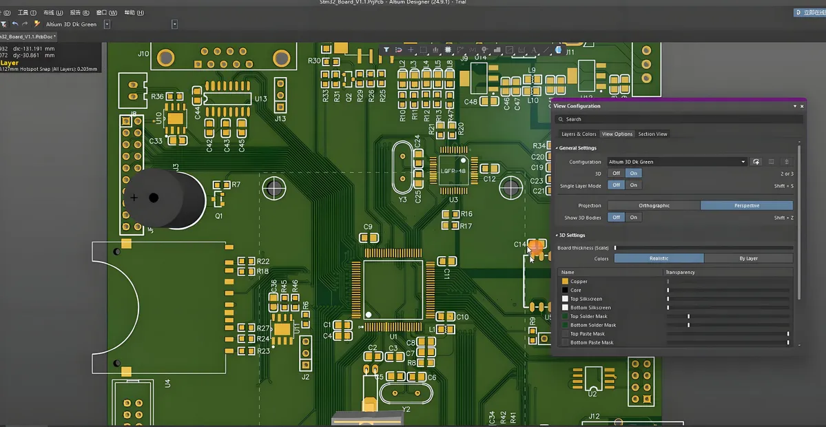
1. Use Design Software Features for Test Point Planning
Modern PCB design tools often include features to automate or assist with test point placement. Leverage these tools to simulate probe access and identify potential issues before sending your design to manufacturing. For instance, set up design rule checks (DRC) to flag test points that violate spacing or accessibility guidelines. This proactive approach can save hours of redesign time.
2. Collaborate with Your Testing Team Early
Engage with your testing team or manufacturing partner during the design phase to understand their specific flying probe equipment capabilities. Some machines may have unique probe sizes or angle limitations (e.g., a minimum probe spacing of 0.4 mm instead of 0.5 mm). Tailoring your design to their setup ensures smoother testing and fewer revisions.
3. Minimize Test Points Without Sacrificing Coverage
While comprehensive testing is crucial, too many test points can slow down the process. Analyze your design to identify critical nets that absolutely need testing (e.g., power rails carrying 5V or high-speed signals at 200 MHz) and reduce redundant points on less critical areas. A balanced approach typically results in a testing time reduction of 20-30% without compromising quality.
4. Document Test Points Clearly in Design Files
Include detailed documentation in your PCB design files, such as a test point map or layer indicating the purpose of each point (e.g., ground, signal, power). This clarity helps the testing team program the flying probe machine more efficiently, reducing setup errors by up to 15% based on industry feedback.
Common Mistakes to Avoid in Design for Flying Probe Testing
Even with the best intentions, certain design oversights can derail your flying probe testing process. Here are some pitfalls to watch out for:
- Ignoring Probe Access on Dense Boards: High-density designs often crowd components, blocking probe paths. Always double-check accessibility, even if it means relocating components or test points.
- Overlooking Solder Mask Issues: Applying solder mask over test points can prevent proper contact. Always specify bare pads in your design files.
- Inconsistent Test Point Sizes: Using test points smaller than 0.8 mm can lead to unreliable contact, especially on boards with slight manufacturing tolerances.
Avoiding these mistakes ensures that your PCB is test-ready from the start, saving time and costs during production.
Benefits of Optimizing for Flying Probe Testing
Investing time in optimizing your PCB for flying probe testing pays off in multiple ways. First, it reduces testing time by up to 25%, as probes can access points quickly and accurately. Second, it lowers the risk of false negatives or positives during testing, ensuring higher product reliability. Finally, a well-designed PCB minimizes the need for costly redesigns or manual testing interventions, streamlining your path from prototype to production.
Final Thoughts on Design for Flying Probe Testing
Creating a PCB that’s optimized for flying probe testing doesn’t have to be complicated. By focusing on flying probe testing accessibility, mastering flying probe testing test point placement, and adhering to essential flying probe testing rules, you can design boards that are easier to test and more reliable in the field. Start with the basics—proper spacing, strategic test point locations, and clear documentation—and build on these with advanced tips like software simulations and early collaboration with your testing team.
At ALLPCB, we’re committed to supporting engineers with resources and services that make PCB design and manufacturing seamless. By applying these strategies for design for flying probe testing, you’ll not only improve your testing outcomes but also bring your products to market faster and with greater confidence.


