 ALLPCB


In the world of high-speed electronics, ensuring signal integrity in printed circuit boards (PCBs) is critical. One advanced technique that plays a major role in this is PCB back drilling. If you're looking for a PCB back drilling tutorial or ways to improve signal integrity in PCB design, you've come to the right place. This guide will walk you through the essentials of back drilling, via stub removal techniques, high-speed PCB layout considerations, and controlled depth drilling. Let’s dive into how mastering these methods can elevate your PCB designs to meet the demands of modern electronics.
What Is PCB Back Drilling and Why Does It Matter?
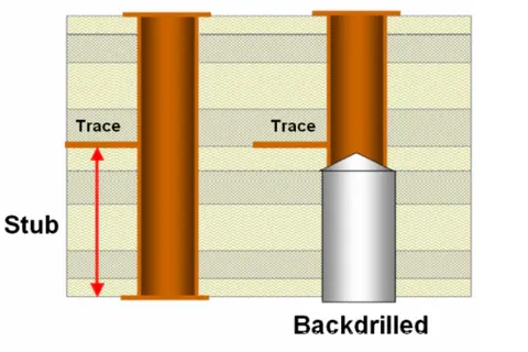
PCB back drilling, also known as controlled depth drilling, is a manufacturing process used to remove unused portions of copper from through-hole vias in a PCB. These unused sections, often called via stubs, can cause signal reflections and degrade signal integrity, especially in high-speed designs. By carefully drilling out these stubs, back drilling minimizes signal loss and ensures cleaner, more reliable data transmission.
In high-speed PCB layouts, where signals travel at gigabit speeds, even small imperfections can lead to significant issues. For instance, a via stub as short as 0.5 mm can introduce enough impedance mismatch to cause signal distortion at frequencies above 5 GHz. Back drilling addresses this problem directly, making it a go-to solution for engineers working on cutting-edge applications like telecommunications, data centers, and advanced computing.
The Basics of Signal Integrity in PCB Design
Before diving deeper into back drilling, it’s important to understand signal integrity in PCB design. Signal integrity refers to the quality of an electrical signal as it travels through a circuit. Poor signal integrity can result in data errors, timing issues, and overall system failure. Factors like impedance mismatches, crosstalk, and reflections from via stubs are common culprits.
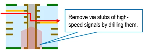
In high-speed designs, signals often operate at frequencies where even tiny structural elements, like a via stub, act as antennas or resonators, disrupting the signal path. This is where via stub removal techniques come into play. By eliminating these problematic stubs through back drilling, you can maintain a consistent impedance—often targeting a standard 50 ohms for many high-speed signals—and ensure the signal reaches its destination without distortion.
How PCB Back Drilling Works: A Step-by-Step Overview
Back drilling is a precise process that requires careful planning and execution during PCB fabrication. Here’s how it typically works:
- Design Planning: During the PCB layout phase, engineers identify vias that will have unused portions (stubs) after the board is assembled. These are usually through-hole vias in multilayer boards where the signal only travels partway through the stackup.
- Drilling Setup: A drill with a slightly larger diameter than the original via hole is used. This ensures that the conductive copper barrel of the stub is completely removed without damaging the functional part of the via.
- Controlled Depth Drilling: The drilling process is controlled to stop at a specific depth, leaving the active signal path intact while removing the stub. Modern fabrication equipment can achieve depth tolerances as tight as ±0.05 mm.
- Inspection: After drilling, the board is inspected to ensure no residual copper remains in the stub area and that the via’s integrity is preserved.
This process is especially critical for multilayer PCBs with 8 or more layers, where via stubs are more likely to occur due to the complexity of signal routing across different layers.
Benefits of Back Drilling for High-Speed PCB Layout
Implementing back drilling in your high-speed PCB layout offers several key advantages. Let’s break them down:
- Improved Signal Integrity: By removing via stubs, back drilling reduces signal reflections and maintains a stable impedance. For example, in a 10 Gbps design, eliminating a 1 mm stub can reduce signal loss by up to 0.5 dB.
- Reduced Crosstalk: Stubs can act as unintended signal paths, causing interference between adjacent traces. Back drilling minimizes this risk, ensuring cleaner signal transmission.
- Support for Higher Frequencies: As data rates climb to 25 Gbps and beyond, back drilling becomes essential to handle the tighter tolerances required for signal fidelity.
- Enhanced Reliability: Cleaner signals mean fewer data errors, leading to more reliable systems, especially in mission-critical applications like aerospace and medical devices.
These benefits make back drilling a powerful tool for engineers aiming to push the boundaries of PCB performance.
Via Stub Removal Techniques: Beyond Back Drilling
While back drilling is the most common method for via stub removal, it’s worth exploring other techniques that can complement or, in some cases, replace it depending on the design constraints:
- Blind and Buried Vias: Instead of drilling through the entire board, blind vias (connecting outer layers to inner layers) or buried vias (connecting only inner layers) can be used to avoid creating stubs in the first place. These are more expensive to manufacture but can be ideal for complex designs.
- Sequential Lamination: This process builds the PCB in stages, allowing vias to be drilled only to the necessary depth during each stage. It’s a more advanced and costly approach but offers precise control over via lengths.
- Stub Tuning: In some cases, stubs can be left in place but tuned to resonate at frequencies outside the signal’s operating range. This requires careful simulation and isn’t always practical for broadband signals.
While these alternatives have their place, back drilling remains the most widely used and cost-effective solution for most high-speed PCB designs.
Best Practices for Implementing Back Drilling in PCB Design
To get the most out of back drilling, follow these best practices during the design and manufacturing stages:
- Simulate Early: Use signal integrity simulation tools to identify problematic vias and predict the impact of stubs on your design. Target impedance mismatches below 5% for critical high-speed lines.
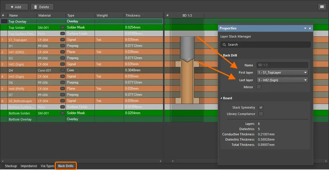
- Collaborate with Fabricators: Work closely with your PCB manufacturer to define back drilling parameters, such as drill depth and tolerance. Ensure they have the capability to handle controlled depth drilling with precision.
- Optimize Layer Stackup: Design your layer stackup to minimize the number of vias that require back drilling. Route high-speed signals on outer layers when possible to reduce stub length.
- Specify Tolerances: Clearly define back drilling depth tolerances in your design files. A common specification is to leave a residual stub of less than 0.2 mm to minimize signal impact.
- Test and Validate: After fabrication, use time-domain reflectometry (TDR) to measure impedance and confirm that stubs have been effectively removed.
Following these steps can help ensure that back drilling delivers the desired improvements in signal integrity without introducing new issues.
Challenges and Limitations of Back Drilling
While back drilling offers significant benefits, it’s not without challenges. Being aware of these limitations can help you plan your design more effectively:
- Increased Cost: Back drilling adds an extra step to the manufacturing process, which can increase production costs by 10-20% depending on the board complexity.
- Design Constraints: Not all vias can be back drilled due to spacing or depth limitations. For instance, vias near components or in dense areas may be inaccessible to drills.
- Potential for Errors: If the drilling depth isn’t controlled precisely, there’s a risk of damaging the active signal path or leaving residual copper that still causes reflections.
Despite these challenges, the advantages of back drilling often outweigh the drawbacks, especially for high-speed applications where signal integrity is non-negotiable.
Controlled Depth Drilling: Precision in Action
Controlled depth drilling is at the heart of effective back drilling. This technique relies on advanced drilling equipment capable of stopping at a predefined depth with high accuracy. Modern CNC drilling machines can achieve depth control within ±0.05 mm, ensuring that only the stub is removed without affecting the functional via.
The success of controlled depth drilling depends on several factors, including the drill bit size, material stackup, and machine calibration. For example, a typical drill bit for back drilling might be 0.1 mm larger than the original via hole to ensure complete stub removal. Fabricators also use specialized software to program drilling depths based on the PCB’s layer stackup, ensuring consistency across thousands of vias on a single board.
Applications of Back Drilling in Modern Electronics
Back drilling is widely used across industries where high-speed data transmission is critical. Some common applications include:
- Telecommunications: High-speed routers and switches operating at 100 Gbps or more rely on back drilling to maintain signal clarity across complex multilayer boards.
- Data Centers: Servers and storage systems use back-drilled PCBs to handle massive data throughput with minimal latency.
- Automotive Electronics: Advanced driver-assistance systems (ADAS) and infotainment systems require reliable high-speed signals for real-time processing.
- Medical Devices: Imaging equipment like MRI machines uses high-frequency signals that benefit from the improved integrity provided by back drilling.
In each of these fields, back drilling helps engineers meet stringent performance standards while pushing the limits of what’s possible with PCB technology.
Conclusion: Elevate Your PCB Designs with Back Drilling
Mastering PCB back drilling is a game-changer for anyone working on high-speed PCB layouts. By understanding the principles of signal integrity in PCB design, leveraging via stub removal techniques like controlled depth drilling, and following best practices, you can create boards that perform reliably even at the highest data rates. Whether you’re designing for telecommunications, data centers, or cutting-edge consumer electronics, back drilling offers a proven way to enhance signal quality and reduce errors.
At ALLPCB, we’re committed to supporting engineers with the tools and expertise needed to bring their designs to life. Incorporating advanced techniques like back drilling into your workflow can set your projects apart in today’s competitive landscape. Start applying these principles to your next design, and experience the difference that precision and signal integrity can make.


