ALLPCB


PCB legend printing, often referred to as silkscreen or overlay, is a critical aspect of printed circuit board design that ensures clarity and functionality. It involves adding text and symbols on the PCB surface to guide assembly, testing, and troubleshooting. Whether you're a seasoned engineer or a newcomer to PCB design, understanding PCB legend design rules, PCB legend readability standards, PCB legend content guidelines, PCB legend best practices, and functional PCB legend printing is essential for creating reliable and user-friendly boards. In this guide, we’ll break down everything you need to know to master PCB legend printing, from fundamental concepts to advanced tips for optimizing design and manufacturability.
What Is PCB Legend Printing and Why Does It Matter?
PCB legend printing is the process of applying identification text, symbols, and patterns onto the surface of a printed circuit board, typically over the soldermask layer. This layer serves as a visual guide for anyone working with the board, whether during assembly, testing, or repair. It includes vital information such as component labels, polarity markers, pin numbers, and even manufacturer logos.
The importance of a well-designed legend cannot be overstated. A clear and functional legend reduces errors during assembly, speeds up troubleshooting, and ensures that the board can be easily understood by multiple stakeholders, from designers to technicians. Poorly designed legends, on the other hand, can lead to costly mistakes, such as incorrect component placement or misinterpretation of connections.
In the following sections, we’ll dive deep into the best practices and guidelines to ensure your PCB legends are both clear and functional, helping you avoid common pitfalls and achieve professional results.
Understanding PCB Legend Design Rules
Designing a PCB legend starts with adhering to specific design rules that ensure the printed text and symbols are manufacturable and effective. These rules are often dictated by the capabilities of the manufacturing process and the need for clarity. Let’s explore some key PCB legend design rules to keep in mind:
- Minimum Text Size: Most manufacturers recommend a minimum text height of 0.8 mm (31 mils) and a line width of 0.15 mm (6 mils) to ensure readability. Smaller text may not print clearly due to limitations in silkscreen printing technology.
- Clearance from Pads and Vias: Legends should maintain a minimum clearance of 0.2 mm (8 mils) from solder pads, vias, and other conductive areas to prevent overlap or interference during assembly.
- Orientation Consistency: Text and symbols should be oriented in a consistent direction, typically readable from a single perspective, to avoid confusion during assembly.
- Layer Specification: Ensure the legend is placed on the correct layer in your design software (often labeled as "Silkscreen" or "Overlay") and separated from other design elements like traces or soldermask.
By following these rules, you can avoid manufacturing issues and ensure that your legend serves its purpose effectively. Always consult your manufacturer’s specific guidelines, as capabilities can vary depending on the equipment and processes used.
Ensuring PCB Legend Readability Standards
Readability is at the heart of a functional PCB legend. If the text and symbols are hard to read, the legend fails to serve its purpose. Here are some PCB legend readability standards to follow:
- Contrast with Background: Use a color that contrasts well with the soldermask. White legends on green, black, or blue soldermask are common choices for high visibility.
- Font Selection: Stick to simple, sans-serif fonts like Arial or Helvetica. Avoid decorative fonts that can distort during printing. A stroke width-to-height ratio of 1:5 is often recommended for clarity.
- Avoid Overcrowding: Leave enough space between text and symbols to prevent them from blending together. A spacing of at least 0.5 mm (20 mils) between elements is a good rule of thumb.
- Limit Text Density: Only include essential information to avoid cluttering the board. Overloading the legend with unnecessary details can make it harder to read.
Testing readability under different lighting conditions can also help ensure that the legend remains clear in real-world scenarios. A readable legend not only aids in assembly but also enhances the overall professionalism of your PCB design.
Following PCB Legend Content Guidelines
The content of your PCB legend is just as important as its design and readability. Including the right information in the right places can make a significant difference in usability. Here are some PCB legend content guidelines to consider:
- Component Identification: Label each component with its reference designator (e.g., R1 for a resistor, C3 for a capacitor) to match the schematic. This helps assemblers place components correctly.
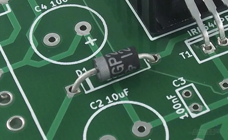
- Polarity and Orientation Marks: For components like diodes, LEDs, and electrolytic capacitors, include polarity markers (e.g., + or -) to indicate correct orientation.
- Pin Numbers: For integrated circuits and connectors, label pin numbers to assist with testing and troubleshooting.
- Board Information: Include details like the board name, version number, and date of design near the edge of the PCB for easy reference.
- Warnings or Instructions: If there are critical handling instructions (e.g., “Handle with ESD precautions”), include them in a visible spot.
While it’s tempting to include as much information as possible, focus on what’s necessary for assembly and maintenance. Too much content can overwhelm users and reduce the legend’s effectiveness.
Adopting PCB Legend Best Practices
Beyond basic rules and guidelines, there are several PCB legend best practices that can elevate the quality of your design. These practices are derived from industry experience and aim to optimize both functionality and aesthetics:
- Prioritize Key Information: Place critical labels, such as polarity markers, closer to the relevant components, while secondary information like board version can be positioned in less prominent areas.
- Use Standard Symbols: Stick to universally recognized symbols for elements like ground, power, or test points to ensure clarity across different teams and regions.
- Account for Assembly Processes: If your board will be assembled by hand, ensure labels are near the components. For automated assembly, focus on labels that assist post-assembly testing.
- Consider Two-Sided Legends: For double-sided PCBs, ensure legends on both sides are consistent and do not overlap with mounting holes or other features.
- Test Print Simulations: Before finalizing your design, use design software to simulate how the legend will appear after printing. This can help catch issues like misalignment or illegible text.
Implementing these best practices can make your PCB legend not only functional but also a mark of professional craftsmanship.
Techniques for Functional PCB Legend Printing
The actual printing of the legend is a crucial step that determines its final quality. Understanding the techniques and limitations of functional PCB legend printing can help you design with manufacturability in mind. Here are some key points to consider:
- Silkscreen Printing: The most common method, silkscreen printing, uses a mesh stencil to apply ink onto the PCB surface. It’s cost-effective for medium to large runs but may struggle with very fine details below 0.15 mm (6 mils).
- Direct Legend Printing: Some modern manufacturers use inkjet-style direct printing, which offers higher precision for small text and complex symbols. This method is ideal for prototypes or small batches but may be more expensive.
- Material Compatibility: Ensure the ink used for legend printing is compatible with the soldermask material and can withstand the assembly process, including soldering temperatures up to 260°C (500°F) and cleaning solvents.
- Resolution Limitations: Work within the resolution limits of the printing process. For silkscreen, a minimum line width of 0.15 mm (6 mils) is standard, while direct printing can sometimes achieve finer details down to 0.1 mm (4 mils).
Choosing the right printing technique depends on your project’s budget, volume, and design complexity. Collaborating closely with your manufacturer can help you select the best method for achieving a high-quality legend.
Common Mistakes to Avoid in PCB Legend Printing
Even with the best intentions, mistakes in PCB legend design and printing can lead to costly errors. Here are some common pitfalls to watch out for:
- Text Too Small: Designing text below the minimum size can result in illegible printing, making the legend useless.
- Overlapping Elements: Placing text too close to pads or vias can cause it to be obscured by solder or components during assembly.
- Inconsistent Orientation: Text oriented in multiple directions can confuse assemblers, leading to placement errors.
- Ignoring Manufacturer Guidelines: Failing to follow your manufacturer’s specific design rules can result in printing defects or delays.
- Cluttered Design: Including too much information can make the legend hard to read and defeat its purpose.
By being mindful of these issues, you can save time and resources while ensuring your PCB legend meets its intended goals.
How to Verify Your PCB Legend Before Manufacturing
Before sending your design for manufacturing, it’s crucial to verify the legend for accuracy and functionality. Here are some steps to follow:
- Review in Design Software: Use your design tool’s 3D view or overlay preview to check for alignment and readability issues.
- Print a Prototype: If possible, print a small batch or prototype to test the legend under real conditions. Check for clarity, contrast, and placement accuracy.
- Get Feedback: Share the design with colleagues or assembly teams to ensure the legend is intuitive and useful from their perspective.
- Check Manufacturer Files: Ensure the legend layer is correctly exported in your Gerber files or other manufacturing outputs to avoid miscommunication with the manufacturer.
Taking these steps can help catch errors early and ensure a smooth manufacturing process.
Conclusion: Mastering PCB Legend Printing for Better Designs
PCB legend printing is a small but vital part of printed circuit board design that directly impacts assembly, testing, and maintenance. By following PCB legend design rules, adhering to PCB legend readability standards, applying PCB legend content guidelines, adopting PCB legend best practices, and understanding functional PCB legend printing techniques, you can create legends that are clear, useful, and professional.
From ensuring minimum text sizes to choosing the right printing method, every detail matters. A well-designed legend not only reduces errors but also enhances the overall quality of your PCB. As you work on your next project, keep these guidelines in mind to achieve optimal results and streamline your workflow.
With the right approach, your PCB legends will serve as a reliable guide for everyone involved in the lifecycle of your board, from design to deployment.