ALLPCB


In the fast-evolving world of electronics, 8-layer PCBs (Printed Circuit Boards) are becoming a cornerstone for high-performance devices. As technology demands more compact, efficient, and powerful systems, the future of 8-layer PCBs is shaped by cutting-edge trends and innovations. From advanced manufacturing techniques to new materials and AI-driven design, the landscape of 8-layer PCB development is transforming rapidly. This blog dives deep into the key advancements, including 8-layer PCB future trends, advanced manufacturing, new materials, miniaturization, and AI in design, to help engineers and designers stay ahead of the curve.
What Are 8-Layer PCBs and Why Do They Matter?
Before exploring future trends, let's understand the basics. An 8 layer PCB is a multilayer board with eight conductive layers stacked with insulating material in between. These boards are used in complex electronics like telecommunications equipment, high-speed computing devices, and advanced medical systems. They offer superior signal integrity, reduced electromagnetic interference (EMI), and the ability to handle dense circuit designs compared to simpler 2- or 4-layer boards.
The importance of 8-layer PCBs lies in their ability to support modern technology's growing needs. With devices becoming smaller yet more powerful, these boards provide the necessary space for intricate routing and high-speed signals, often exceeding 5 GHz in applications like 5G infrastructure. As we look to the future, innovations in design and manufacturing are set to make 8-layer PCBs even more critical to industries worldwide.

Key Trends Shaping the Future of 8-Layer PCBs
The electronics industry is driven by innovation, and 8-layer PCBs are no exception. Below, we explore the most impactful trends that are redefining how these boards are designed and manufactured.
1. 8-Layer PCB Miniaturization: Packing More Power into Smaller Spaces
Miniaturization is a major focus in electronics, and 8-layer PCBs play a vital role in this trend. As devices like smartphones, wearables, and IoT gadgets shrink in size, the demand for compact yet powerful circuit boards grows. Miniaturization in 8-layer PCBs involves reducing the board's footprint while maintaining or even increasing functionality.
One approach to miniaturization is the use of microvias, tiny holes with diameters as small as 0.1 mm, to connect layers. These allow for denser routing, enabling designers to fit more components into a smaller area. Additionally, advancements in surface-mount technology (SMT) have reduced component sizes, with some resistors and capacitors now measuring just 0.4 mm x 0.2 mm. This trend directly impacts 8-layer PCB layouts, allowing for intricate designs without sacrificing performance.
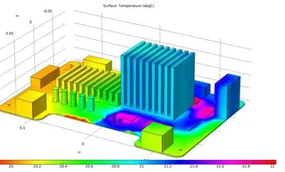
The challenge lies in managing heat dissipation and signal integrity in such compact designs. Future innovations in PCB thermal management, such as embedded heat sinks and advanced dielectric materials, will be crucial for miniaturized 8-layer PCBs to perform reliably in high-power applications.

2. 8-Layer PCB New Materials: Enhancing Performance and Durability
Materials are at the heart of PCB performance, and the future of 8-layer PCBs is tied to the development of new, high-performance materials. Traditional FR-4, while cost-effective, often falls short in high-frequency and high-temperature environments. This has led to the adoption of advanced materials tailored for 8-layer PCB applications.
For instance, high-frequency laminates like PTFE (polytetrafluoroethylene) and ceramic-filled materials are gaining traction. These materials offer low dielectric constants (Dk) around 2.2 to 3.5, compared to FR-4's 4.5, ensuring better signal integrity at frequencies above 10 GHz. Additionally, thermally conductive substrates are being developed to handle heat dissipation in densely packed 8-layer designs, with thermal conductivity values reaching up to 3 W/m·K.
Another exciting development is the use of eco-friendly materials. As sustainability becomes a priority, manufacturers are exploring bio-based resins and halogen-free options to reduce environmental impact without compromising on performance. These new materials will shape the next generation of 8-layer PCBs, making them more robust, efficient, and sustainable.
3. 8-Layer PCB Advanced Manufacturing: Precision and Efficiency
Manufacturing techniques for 8-layer PCBs are evolving to meet the demands of complexity and precision. Advanced manufacturing focuses on improving layer alignment, reducing defects, and speeding up production while maintaining high quality.
Laser drilling is one such innovation, allowing for the creation of microvias with extreme accuracy. This method achieves hole sizes as small as 0.075 mm, compared to traditional mechanical drilling's limit of around 0.2 mm. This precision is critical for 8-layer PCBs, where even a slight misalignment can disrupt signal paths and cause failures.
Another trend is the adoption of additive manufacturing, or 3D printing, for prototyping 8-layer PCBs. This technology enables rapid iteration of designs, reducing lead times from weeks to days. Furthermore, automated optical inspection (AOI) systems are being integrated into production lines to detect defects like open circuits or shorts with a resolution of up to 10 micrometers, ensuring flawless boards for high-stakes applications.
As manufacturing becomes more advanced, costs are expected to decrease, making 8-layer PCBs more accessible for a wider range of industries, from automotive to aerospace.

4. 8-Layer PCB AI in Design: Smarter and Faster Development
Artificial Intelligence (AI) is revolutionizing the way 8-layer PCBs are designed. With the increasing complexity of multilayer boards, manual design processes are becoming time-consuming and prone to errors. AI steps in to streamline workflows, optimize layouts, and predict potential issues before manufacturing begins.
AI-powered design tools can analyze millions of routing possibilities in seconds, identifying the most efficient paths for signals while minimizing crosstalk and EMI. For example, these tools can maintain impedance values within tight tolerances, such as ±5% for high-speed signals, ensuring reliable performance. Additionally, AI can simulate thermal behavior, predicting hotspots in an 8-layer PCB design with accuracy down to 0.1°C, allowing engineers to address cooling needs early in the process.
Beyond design optimization, AI is also being used for predictive maintenance in manufacturing. By analyzing data from production equipment, AI systems can forecast when machines might fail, reducing downtime and ensuring consistent output of high-quality 8-layer PCBs. As AI technology matures, its integration into PCB design software will become even more seamless, empowering engineers to create cutting-edge solutions faster than ever.
5. 8-Layer PCB Future Trends: What Lies Ahead?
Looking beyond current advancements, several emerging trends are poised to shape the long-term future of 8-layer PCBs. One such trend is the integration of embedded components. By embedding passive components like resistors and capacitors directly into the layers of an 8-layer PCB, designers can save surface space and improve signal integrity by reducing parasitic effects. This technology is still in its early stages but is expected to become mainstream within the next 5-10 years.
Another promising area is the rise of flexible and rigid-flex 8-layer PCBs. These boards combine the benefits of multilayer complexity with the adaptability of flexible materials, making them ideal for wearable electronics and compact medical devices. Innovations in flexible substrates with dielectric constants as low as 2.5 are already showing potential for high-frequency applications.
Finally, the push for 5G and beyond will continue to drive 8-layer PCB development. With signal speeds exceeding 25 Gbps in next-generation networks, PCBs must support ultra-low latency and minimal signal loss. This will require ongoing advancements in materials, manufacturing precision, and design tools to keep pace with the demands of future connectivity standards.
Benefits of These Innovations for Engineers and Industries
The trends and innovations discussed above bring tangible benefits to engineers and the industries they serve. Miniaturization allows for the creation of smaller, lighter devices without sacrificing performance, which is crucial for consumer electronics and portable medical equipment. New materials enhance durability and signal quality, ensuring that 8-layer PCBs can withstand harsh environments in automotive and industrial applications.
Advanced manufacturing reduces production errors and speeds up time-to-market, giving companies a competitive edge. Meanwhile, AI in design minimizes human error and accelerates the development cycle, enabling engineers to focus on innovation rather than repetitive tasks. Collectively, these advancements make 8-layer PCBs more reliable, cost-effective, and adaptable to a wide range of applications.
Challenges to Overcome in 8-Layer PCB Development
While the future of 8-layer PCBs is bright, there are challenges to address. The complexity of multilayer designs increases the risk of manufacturing defects, requiring stricter quality control measures. Miniaturization, while beneficial, can lead to overheating if thermal management isn’t optimized. Additionally, the cost of adopting new materials and technologies may be prohibitive for smaller companies, at least in the short term.
However, as technology advances and economies of scale come into play, these challenges are likely to diminish. Collaboration between material scientists, engineers, and manufacturers will be key to overcoming hurdles and ensuring that 8-layer PCBs continue to meet the needs of tomorrow’s electronics.
Conclusion: Preparing for the Future of 8-Layer PCBs
The future of 8-layer PCBs is defined by exciting trends and innovations that promise to push the boundaries of what’s possible in electronics. From miniaturization and new materials to advanced manufacturing and AI-driven design, these advancements are transforming how 8-layer PCBs are created and used. By staying informed about 8-layer PCB future trends, engineers and designers can leverage these developments to build more efficient, reliable, and compact solutions for a variety of industries.
At ALLPCB, we’re committed to supporting the evolution of PCB technology by providing cutting-edge solutions and resources for multilayer designs. Whether you’re working on high-speed telecommunications equipment or compact IoT devices, understanding and adopting these trends will help you stay ahead in a competitive landscape. The journey of 8-layer PCB innovation is just beginning, and the possibilities are endless.