 ALLPCB


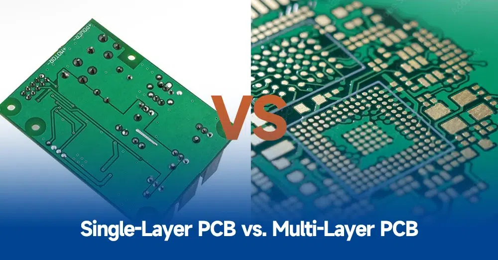
In the fast-evolving world of electronics, choosing the right printed circuit board (PCB) design is crucial for performance, cost, and efficiency. Single-layer PCBs, also known as single-sided PCBs, are among the simplest and most cost-effective options available. But what are the single layer PCB advantages and single layer PCB limitations? When should you use a single-layer PCB over more complex multi-layer designs? In this comprehensive guide, we’ll explore the pros and cons of single-sided PCBs, key PCB design considerations, and practical scenarios for their use in modern electronics.
Whether you’re an engineer working on a basic prototype or a designer looking to optimize costs, understanding the single sided PCB pros and cons can help you make informed decisions. Let’s dive into the details of single-layer PCBs and uncover how they fit into today’s electronic design landscape.
What Is a Single-Layer PCB?
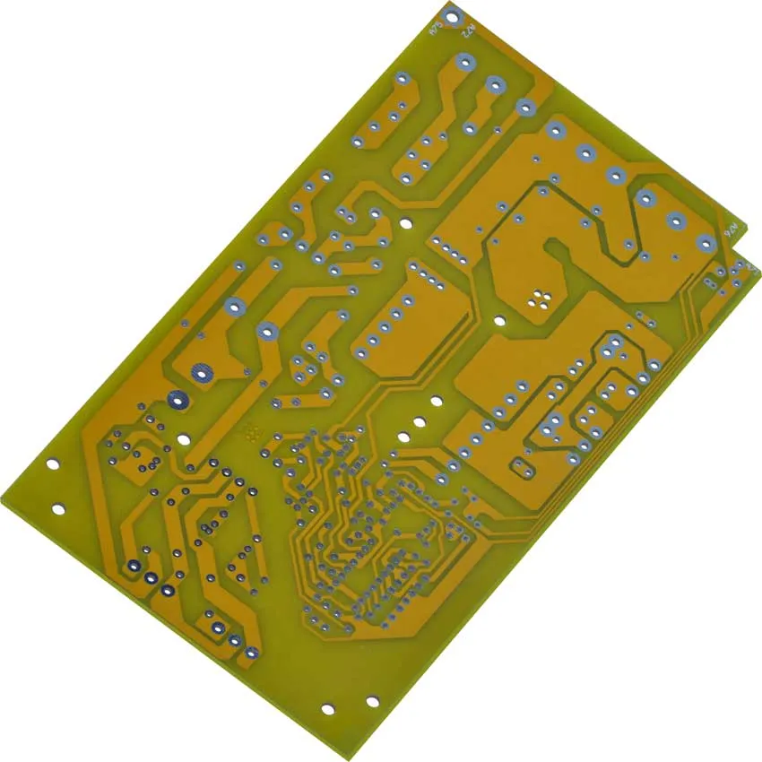
A single-layer PCB is a type of printed circuit board that has conductive copper traces on only one side of the board. The other side typically holds the components, which are soldered to the traces through holes or surface-mount technology. These boards are the most basic form of PCB and have been used for decades in simple electronic devices.
Due to their straightforward design, single-layer PCBs are often the go-to choice for low-complexity projects. They are widely used in applications like calculators, LED lighting, and basic power supplies. However, as electronics become more advanced, their role is often limited to specific use cases. To understand if a single-layer PCB is right for your project, let’s break down the single layer PCB advantages and limitations.
Advantages of Single-Layer PCBs in Modern Electronics
Single-layer PCBs offer several benefits that make them a viable option for certain applications. Below, we’ll explore the key single layer PCB advantages that engineers and designers can leverage.
1. Cost-Effectiveness
One of the most significant benefits of single-layer PCBs is their low cost. Since they use fewer materials and require simpler manufacturing processes compared to multi-layer boards, they are much cheaper to produce. For small-scale projects or mass production of basic devices, this cost advantage can save substantial amounts. For example, producing a single-layer PCB can cost as little as 30-50% of a double-layer board for the same size, depending on the design and volume.
2. Simplicity in Design and Manufacturing
The design of a single-layer PCB is straightforward, with all traces confined to one side. This simplicity reduces the chances of errors during the design phase and speeds up the manufacturing process. For engineers working on basic circuits with fewer components, this means faster prototyping and quicker time-to-market. Software tools for PCB layout can easily handle single-layer designs without the need for complex routing algorithms.
3. Easier Testing and Repair
With traces and components visible on just one side, single-layer PCBs are easier to test and troubleshoot. If a circuit fails, identifying a broken trace or faulty component is often as simple as a visual inspection or using a multimeter. Repairs are also less complicated since there are no hidden layers to navigate. This advantage is particularly useful for educational projects or hobbyist electronics where frequent modifications are common.

4. Ideal for Low-Density Designs
Single-layer PCBs are perfect for low-density designs where the number of connections and components is minimal. For instance, a basic LED driver circuit or a simple timer might only require a handful of traces, making a single-layer board more than sufficient. This avoids the unnecessary expense and complexity of multi-layer boards for projects that don’t need advanced functionality.
5. Faster Production Times
Since single-layer PCBs involve fewer manufacturing steps, such as no need for layer alignment or via drilling between layers, production times are significantly shorter. This can be a critical factor for projects with tight deadlines or when rapid iterations are needed during the development phase.
Limitations of Single-Layer PCBs in Modern Electronics
While single-layer PCBs have clear benefits, they also come with notable drawbacks. Understanding these single layer PCB limitations is essential for deciding if they are suitable for your project.
1. Limited Complexity and Functionality
The biggest limitation of single-layer PCBs is their inability to handle complex circuits. With traces restricted to one side, there’s a finite amount of space for connections. As modern electronics often require high-density designs with numerous components, single-layer boards quickly become impractical. For example, a smartphone or computer motherboard would be impossible to design on a single layer due to the thousands of connections needed.
2. Slower Speed and Lower Operating Capacity
Single-layer PCBs are not ideal for high-speed applications. The limited space for traces often leads to longer signal paths, which can increase impedance and result in slower signal transmission. For instance, in a high-frequency circuit operating at 1 GHz, signal integrity issues like crosstalk and noise become more pronounced on a single-layer board compared to a multi-layer design with dedicated ground planes.
3. Larger Physical Size
To accommodate all necessary traces on one side, single-layer PCBs often need to be larger in size compared to multi-layer boards that can stack connections vertically. This can be a disadvantage in modern electronics where miniaturization is a priority. A device like a wearable fitness tracker, for example, would struggle to fit a single-layer PCB due to space constraints.
4. Poor EMI and Signal Integrity
Electromagnetic interference (EMI) is a common issue with single-layer PCBs. Without additional layers for grounding or shielding, these boards are more susceptible to noise, especially in environments with multiple electronic devices. This limitation makes them less suitable for sensitive applications like medical equipment or RF communication devices where signal integrity is critical.
When to Use Single-Layer PCBs
Deciding when to use single layer PCB designs depends on the specific needs of your project. Here are some scenarios where single-layer PCBs are the best choice:
- Basic Electronics Projects: For simple devices like alarms, basic sensors, or small power supplies, single-layer PCBs provide a cost-effective and practical solution.
- Prototyping and Education: Hobbyists, students, and engineers testing initial concepts often use single-layer PCBs due to their simplicity and ease of modification.
- Cost-Sensitive Products: In mass-produced items where cost is a primary concern—such as low-end consumer electronics—single-layer PCBs help keep expenses down.
- Low-Speed Applications: If your circuit operates at low frequencies (e.g., below 100 kHz) and doesn’t require complex routing, a single-layer board is often sufficient.
On the other hand, if your project involves high-speed signals, dense component placement, or strict size constraints, a multi-layer PCB might be necessary despite the higher cost.
PCB Design Considerations for Single-Layer Boards
When designing a single-layer PCB, several PCB design considerations must be kept in mind to ensure functionality and reliability. Below are key factors to focus on:
1. Trace Routing and Spacing
Since all traces are on one side, routing can become challenging as the number of connections increases. Ensure adequate spacing between traces to prevent short circuits and minimize crosstalk. A common rule of thumb is to maintain at least 6 mils (0.006 inches) of spacing for standard designs, though this may vary based on voltage and current requirements.
2. Component Placement
Place components strategically to minimize trace length and avoid congestion. Grouping related components together can reduce the need for long traces, improving signal performance and reducing potential interference.
3. Heat Dissipation
Single-layer PCBs lack additional layers for heat distribution, so consider adding heat sinks or wider copper areas for components that generate significant heat, such as power transistors or voltage regulators. Poor heat management can lead to component failure or reduced lifespan.
4. Use of Jumpers
In some cases, traces may need to cross each other, which isn’t possible on a single-layer board without breaking continuity. Using jumper wires or zero-ohm resistors can solve this issue, though it adds to assembly time and potential points of failure.

Single-Sided PCB Pros and Cons: A Quick Summary
To wrap up the key points, here’s a concise overview of the single sided PCB pros and cons:
Pros:
- Low cost for design and manufacturing.
- Simple and quick to produce.
- Easy to test and repair.
- Suitable for low-density, low-speed applications.
Cons:
- Limited to basic, low-complexity circuits.
- Poor performance in high-speed or high-frequency applications.
- Larger size compared to multi-layer boards.
- Higher susceptibility to EMI and noise.
How Single-Layer PCBs Fit Into Modern Electronics
In today’s world of compact, high-performance electronics, single-layer PCBs may seem outdated at first glance. Devices like smartphones, laptops, and IoT gadgets often rely on multi-layer boards with 4, 6, or even 8 layers to handle intricate designs and high-speed data transfer. However, single-layer PCBs still hold a vital place in the industry for specific applications.
For example, in rural or developing regions, low-cost electronics like solar-powered lanterns or basic radios often use single-layer PCBs to keep production costs minimal. Similarly, in educational settings, these boards are invaluable for teaching fundamental electronics concepts due to their simplicity.
Moreover, as sustainability becomes a focus in electronics manufacturing, the reduced material usage of single-layer PCBs can contribute to less waste compared to complex multi-layer designs. While they can’t meet the demands of cutting-edge technology, their niche role ensures they remain relevant.
Conclusion: Making the Right Choice for Your Project
Single-layer PCBs offer a practical solution for many electronics projects, balancing cost, simplicity, and functionality. Their single layer PCB advantages—like affordability and ease of use—make them ideal for basic applications, prototyping, and cost-sensitive products. However, their single layer PCB limitations—such as restricted complexity and poor performance in high-speed scenarios—mean they aren’t suitable for every design.
By carefully considering your project’s requirements and the PCB design considerations outlined above, you can determine when to use single layer PCB designs effectively. Whether you’re building a simple circuit or exploring initial concepts, single-layer PCBs can be a valuable tool in your engineering toolkit.
At ALLPCB, we’re committed to supporting your PCB needs, from single-layer designs to complex multi-layer boards. With a focus on quality and efficiency, we help bring your ideas to life with precision and reliability. Explore our services to see how we can assist with your next project.


