 ALLPCB


If you're looking to design a printed circuit board (PCB) with a 1 oz copper weight and need guidance on optimizing the stackup, you're in the right place. A well-designed PCB stackup with 1 oz copper ensures signal integrity, thermal management, and cost efficiency, whether you're working on a 4-layer or 6-layer board. In this guide, we'll dive deep into the essentials of 1 oz copper PCB stackup, including layer arrangements for 4-layer and 6-layer designs, impedance control strategies, and practical tips for optimization.
Whether you're a beginner or an experienced engineer, this comprehensive resource will walk you through the key considerations for designing an effective PCB layer stackup with 1 oz copper. Let's explore how to achieve the best performance for your electronic projects.
What Is 1 oz Copper in PCB Design?
In PCB manufacturing, copper weight refers to the thickness of the copper layer on each board layer, measured in ounces per square foot (oz/ft2). A 1 oz copper layer means that one square foot of the copper foil weighs 1 ounce, translating to a thickness of approximately 1.4 mils (0.0014 inches or 35 micrometers). This is the industry standard for many PCB designs due to its balance of cost, conductivity, and manufacturability.
Using 1 oz copper in a PCB stackup offers several advantages, including sufficient current-carrying capacity for most low-to-medium power applications and compatibility with standard manufacturing processes. It is widely used in consumer electronics, industrial controls, and communication devices. However, optimizing the stackup design is crucial to ensure performance, especially when dealing with multilayer boards and impedance control requirements.
Why Optimize PCB Stackup with 1 oz Copper?
The stackup of a PCB refers to the arrangement of copper layers and insulating materials (dielectrics) that make up the board. A well-optimized PCB layer stackup with 1 oz copper can significantly impact signal integrity, electromagnetic interference (EMI), thermal performance, and overall reliability. Here are some reasons why optimization matters:
- Signal Integrity: Proper layer arrangement reduces crosstalk and ensures consistent impedance for high-speed signals.
- Power Distribution: Dedicated power and ground planes help minimize voltage drops and noise.
- Thermal Management: Balanced copper distribution prevents hotspots and improves heat dissipation.
- Cost Efficiency: Optimizing layer count and copper usage avoids unnecessary expenses while meeting design needs.
For designs using 1 oz copper, achieving these benefits requires careful planning of layer order, dielectric thickness, and trace geometry, especially in multilayer boards like 4-layer and 6-layer configurations.
Key Considerations for 1 oz Copper PCB Stackup Design
Before diving into specific stackup configurations, let’s cover the fundamental aspects to consider when designing a PCB with 1 oz copper. These principles apply to any multilayer board and are essential for achieving optimal performance.
1. Layer Count and Functionality
Decide on the number of layers based on your circuit complexity. A 4-layer PCB is often sufficient for simpler designs with moderate routing density, while a 6-layer PCB is better suited for high-speed or high-density applications requiring additional signal or power planes.
2. Dielectric Material and Thickness
The dielectric material between copper layers (often FR-4 for standard designs) affects signal speed and impedance. Typical dielectric thickness for 1 oz copper boards ranges from 0.2 mm to 0.8 mm, depending on the layer count and impedance requirements. Thinner dielectrics are often used for tighter impedance control in high-speed designs.
3. Impedance Control
For high-speed signals, maintaining a specific characteristic impedance (e.g., 50 ohms for RF applications) is critical. With 1 oz copper, trace width and spacing, along with dielectric thickness, must be calculated precisely to achieve the desired impedance. Tools like impedance calculators or simulation software can help in this process.
4. Thermal and Mechanical Stability
Ensure that the 1 oz copper layers are balanced across the board to prevent warping during manufacturing or operation. Uneven copper distribution can lead to mechanical stress, especially in multilayer designs.
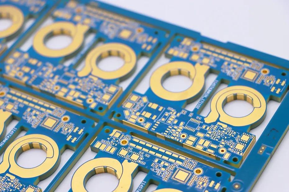
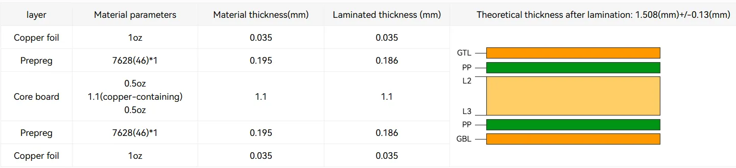
4-Layer PCB Stackup with 1 oz Copper
A 4-layer PCB stackup with 1 oz copper is one of the most common configurations for designs requiring a balance between complexity and cost. It typically includes two signal layers and two plane layers (power and ground). Here’s a standard arrangement for a 4-layer PCB stackup with 1 oz copper:
- Layer 1 (Top): Signal layer for routing traces and components (1 oz copper)
- Layer 2: Ground plane (1 oz copper)
- Layer 3: Power plane (1 oz copper)
- Layer 4 (Bottom): Signal layer for additional routing (1 oz copper)
Dielectric Thickness: The spacing between layers is typically around 0.2-0.3 mm for the prepreg (insulating material between copper layers) to maintain a total board thickness of 1.6 mm, which is a common standard.
Benefits of This 4-Layer Stackup
- Signal Integrity: The ground plane on Layer 2 provides a return path for signals on Layer 1, reducing noise and crosstalk.
- Power Distribution: Dedicated power and ground planes ensure stable voltage delivery.
- Cost-Effective: A 4-layer board is less expensive than higher layer counts while still supporting complex designs.
Impedance Control in 4-Layer PCB with 1 oz Copper
For impedance control in a 4-layer PCB stackup with 1 oz copper, achieving a 50-ohm characteristic impedance for high-speed traces often requires a trace width of approximately 6-8 mils (0.15-0.2 mm) on the top and bottom layers, with a dielectric thickness of 0.2 mm between the signal layer and ground plane. These values can vary based on the dielectric constant of the material (typically 4.2-4.5 for FR-4).
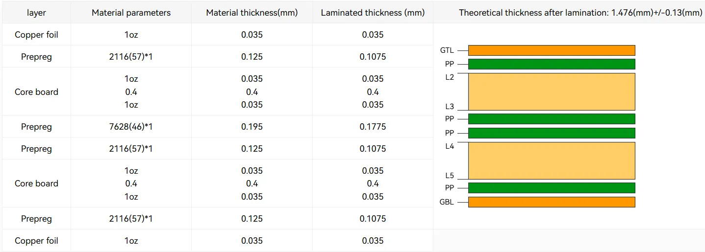
6-Layer PCB Stackup with 1 oz Copper
A 6-layer PCB stackup with 1 oz copper is ideal for more complex designs that require additional routing space or enhanced signal integrity through multiple ground planes. A common configuration for a 6-layer stackup is as follows:
- Layer 1 (Top): Signal layer for high-speed traces (1 oz copper)
- Layer 2: Ground plane (1 oz copper)
- Layer 3: Signal layer for internal routing (1 oz copper)
- Layer 4: Power plane (1 oz copper)
- Layer 5: Ground plane (1 oz copper)
- Layer 6 (Bottom): Signal layer for additional routing (1 oz copper)
Dielectric Thickness: The spacing between layers is often around 0.2 mm for prepreg layers, with a total board thickness of 1.6 mm to 2.0 mm, depending on design requirements.
Benefits of This 6-Layer Stackup
- Enhanced Signal Integrity: Multiple ground planes (Layers 2 and 5) shield signal layers, reducing EMI and crosstalk for high-speed designs.
- Flexible Routing: Additional signal layers (Layers 3 and 6) provide more space for complex trace layouts.
- Power Stability: A dedicated power plane ensures consistent voltage distribution across the board.
Impedance Control in 6-Layer PCB with 1 oz Copper
For impedance control in a 6-layer PCB stackup with 1 oz copper, high-speed traces on Layers 1 and 6 can be designed for 50-ohm impedance by adjusting trace width to around 6-7 mils (0.15-0.18 mm) with a dielectric thickness of 0.2 mm to the nearest ground plane. Internal signal layers (like Layer 3) may require slightly wider traces (8-10 mils) due to their proximity to other planes, depending on the dielectric properties.
Impedance Control Strategies for 1 oz Copper PCB
Impedance control is a critical aspect of high-speed PCB design, especially for applications like RF, USB, or Ethernet. With 1 oz copper, achieving the desired impedance (often 50 ohms or 75 ohms) requires precise control over trace geometry and layer spacing. Here are some strategies to ensure proper impedance control in a 1 oz copper PCB stackup:
1. Calculate Trace Width and Spacing
Use an impedance calculator or simulation tool to determine the trace width and spacing for your target impedance. For a 50-ohm single-ended trace on a 1 oz copper layer with FR-4 dielectric (dielectric constant of 4.3), a trace width of 6-8 mils and a dielectric thickness of 0.2 mm to the reference plane are typical starting points.
2. Maintain Consistent Dielectric Thickness
Work with your PCB manufacturer to ensure uniform dielectric thickness across layers. Variations in thickness can lead to impedance mismatches, affecting signal performance.
3. Use Reference Planes
Always route high-speed signals adjacent to a ground or power plane to provide a stable return path. In both 4-layer and 6-layer stackups with 1 oz copper, ensure that signal layers are close to a reference plane to minimize loop inductance.
4. Minimize Via Effects
Vias can introduce impedance discontinuities. Use back-drilling or blind vias for high-speed signals to reduce stub effects, and keep via counts to a minimum on critical traces.
Tips for Optimizing 1 oz Copper PCB Stackup
Beyond layer arrangement and impedance control, here are some practical tips to further optimize your PCB stackup with 1 oz copper:
- Balance Copper Distribution: Ensure that copper is evenly distributed across layers to prevent board warping during manufacturing or under thermal stress.
- Prioritize Ground Planes: Place ground planes near signal layers to reduce noise and improve signal return paths, especially in high-speed designs.
- Optimize Via Placement: Minimize the use of vias in high-speed signal paths, and place them strategically to avoid interference with critical traces.
- Simulate Before Manufacturing: Use PCB design software to simulate signal integrity and impedance before finalizing your stackup. This can help identify potential issues early.
- Consult with Manufacturers: Collaborate with your PCB fabrication team to confirm that your stackup design aligns with their capabilities, especially for custom dielectric thicknesses or tight impedance tolerances.
Common Challenges and Solutions in 1 oz Copper PCB Stackup Design
Designing a PCB stackup with 1 oz copper can present challenges, especially for multilayer boards or high-speed applications. Here are some common issues and how to address them:
Challenge 1: Signal Crosstalk
Solution: Increase spacing between high-speed traces and use ground planes to isolate signal layers. In a 6-layer stackup, dedicate internal layers to ground to create a shielding effect.
Challenge 2: Thermal Imbalance
Solution: Distribute copper evenly across layers by adding dummy fills or balancing trace density. This prevents warping and improves thermal dissipation.
Challenge 3: Impedance Mismatch
Solution: Use precise calculations for trace width and dielectric thickness, and verify impedance with test coupons during manufacturing to ensure consistency.
Conclusion
Optimizing a PCB stackup for 1 oz copper is a critical step in designing reliable and high-performing electronic circuits. Whether you're working on a 4-layer PCB stackup with 1 oz copper for a cost-effective solution or a 6-layer PCB stackup with 1 oz copper for complex, high-speed applications, understanding layer arrangement, impedance control, and thermal management is essential. By following the guidelines and configurations outlined in this guide, you can achieve a balanced design that meets your performance and cost requirements.
Remember that every project is unique, so tailor your PCB layer stackup with 1 oz copper to the specific needs of your application. With careful planning and collaboration with your manufacturing partner, you can ensure a successful outcome for your next PCB design. Start optimizing your 1 oz copper PCB stackup today for better signal integrity, power stability, and overall board performance.


