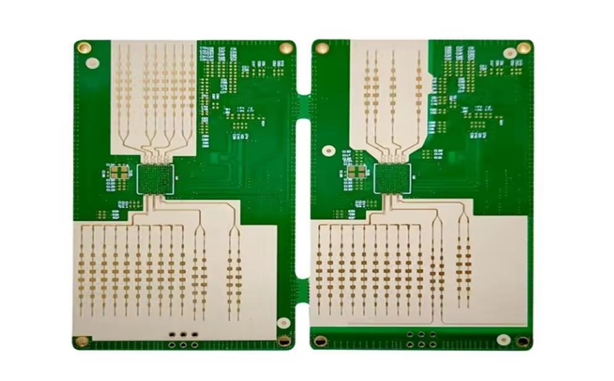
For PCB designers, understanding copper thickness is crucial for creating reliable and efficient circuit boards. Whether you're searching for a PCB copper thickness guide, need help with mils to oz conversion, or want to master copper weight in PCB design, this blog is your go-to resource. Copper thickness directly impacts current capacity, heat dissipation, and signal integrity. In this guide, we'll break down the essentials, from converting copper thickness between mils and ounces to calculating trace thickness for optimal performance. Let's dive into the details to help you design better PCBs with confidence.
Why Copper Thickness Matters in PCB Design
Copper thickness is a foundational aspect of PCB design that affects nearly every performance metric of a circuit board. It determines how much current a trace can carry, how much heat it can dissipate, and how well signals travel without interference. For engineers working on high-power applications or high-speed digital circuits, selecting the right copper thickness is not just a choice—it's a necessity.
In simple terms, copper thickness refers to the amount of copper used on the conductive layers of a PCB. Thicker copper can handle more current and offers better thermal management, while thinner copper is often used for finer traces in compact designs. However, choosing the wrong thickness can lead to issues like overheating, signal loss, or even board failure. This guide will walk you through the practical aspects of copper thickness, with a focus on measurements in mils (thousandths of an inch), conversions to ounces per square foot (oz/ft2), and design considerations for signal integrity.
Understanding Copper Thickness: Mils vs. Ounces
Copper thickness in PCB design is typically measured in two units: ounces per square foot (oz/ft2) and mils (thousandths of an inch). While ounces refer to the weight of copper spread over a square foot, mils describe the actual physical thickness. Let's break down these units and how to convert between them.
What Does 1 Oz of Copper Mean?
When we say "1 oz of copper," it means that 1 ounce of copper is spread evenly over a 1-square-foot area of the PCB. This translates to a physical thickness of approximately 1.37 mils, or 0.00137 inches. This measurement comes from the density of copper and is a standard in the industry for defining copper weight in PCB design.
- 1 oz/ft2 = 1.37 mils
- 2 oz/ft2 = 2.74 mils
- 0.5 oz/ft2 = 0.685 mils
This conversion is essential for designers who need to specify copper thickness in mils for manufacturing or simulation tools but are given requirements in ounces.
Mils to Oz Conversion: A Quick Reference
Converting between mils and ounces is straightforward once you know the baseline. Here's a simple formula for mils to oz conversion:
Copper Weight (oz/ft2) = Thickness (mils) / 1.37
For example, if you have a copper thickness of 2.74 mils, divide by 1.37 to get 2 oz/ft2. This quick calculation helps designers ensure they're meeting the right specifications for their board's needs.
Standard Copper Thicknesses in PCB Manufacturing
In PCB manufacturing, copper thickness typically ranges from 0.5 oz/ft2 to 4 oz/ft2 or more, depending on the application. Here's a breakdown of common thicknesses and their uses:
- 0.5 oz/ft2 (0.685 mils): Often used for inner layers of multilayer boards where space and weight are critical. Best for low-current applications.
- 1 oz/ft2 (1.37 mils): The industry standard for most general-purpose PCBs. It offers a good balance between current capacity and cost.
- 2 oz/ft2 (2.74 mils): Used in power electronics or applications requiring higher current carrying capacity and better heat dissipation.
- 3 oz/ft2 and above (4.11 mils+): Known as heavy copper, used in high-power applications like automotive or industrial systems where traces must handle significant current without overheating.
Choosing the right thickness depends on your design requirements, including current load, thermal management, and manufacturing constraints. Always consult with your fabrication house to ensure they can support your chosen copper weight.
PCB Trace Thickness Calculation: Balancing Current and Width
One of the most critical aspects of PCB design is calculating trace thickness and width to handle the required current without overheating. The current-carrying capacity of a trace depends on its cross-sectional area, which is determined by both the copper thickness and the trace width.
Using IPC-2221 Standards for Trace Width Calculation
The IPC-2221 standard provides guidelines for determining trace width based on current, copper thickness, and allowable temperature rise. For example, a 10-mil-wide trace with 1 oz/ft2 copper (1.37 mils thick) can carry approximately 1 ampere of current with a 10°C temperature rise. If you increase the trace width to 50 mils, the current capacity increases significantly, often exceeding 5 amperes under the same conditions.
To calculate the required trace width for a specific current, you can use online calculators or refer to charts based on IPC-2221. The general rule is that thicker copper and wider traces can handle more current. However, space constraints in compact designs often limit trace width, making copper thickness a critical factor.
Formula for Cross-Sectional Area:
Cross-Sectional Area (mil2) = Trace Width (mils) × Copper Thickness (mils)
For instance, a 20-mil-wide trace with 2 oz/ft2 copper (2.74 mils thick) has a cross-sectional area of 54.8 mil2, which can handle higher currents than a thinner or narrower trace.
Copper Thickness for Signal Integrity in High-Speed Designs
In high-speed PCB designs, copper thickness plays a significant role in maintaining signal integrity. Signal integrity refers to the quality of an electrical signal as it travels through a trace, avoiding issues like crosstalk, reflections, or impedance mismatches.
How Copper Thickness Impacts Impedance
In high-frequency applications, the characteristic impedance of a trace must be controlled to match the source and load impedance, often 50 ohms for RF designs. Copper thickness affects the dielectric spacing between layers and the trace's geometry, both of which influence impedance. Thinner copper allows for finer traces and tighter spacing, which can increase capacitance and lower impedance. Conversely, thicker copper might require wider traces or adjusted dielectric thickness to achieve the desired impedance.
For example, in a microstrip design with a 1.6 mm substrate and 1 oz/ft2 copper (1.37 mils), a trace width of approximately 50 mils might achieve a 50-ohm impedance. If you switch to 2 oz/ft2 copper (2.74 mils), the trace width or dielectric thickness may need adjustment to maintain the same impedance.
Balancing Thickness for Signal Speed and Loss
Thicker copper can reduce resistive losses in traces, which is beneficial for maintaining signal strength over long distances. However, it can also increase parasitic capacitance in densely packed designs, potentially slowing down signal speeds. For high-speed digital signals operating at 1 GHz or above, designers often use thinner copper (like 0.5 oz/ft2 or 0.685 mils) on inner layers to minimize capacitance while using thicker copper on power planes for better current handling.
Practical Tips for Choosing Copper Thickness in Your PCB Design
Selecting the right copper thickness is a balancing act between performance, cost, and manufacturability. Here are some practical tips to guide your decision:
- Start with Application Needs: Determine the current requirements, thermal constraints, and signal speeds of your design. High-power applications often need 2 oz/ft2 or more, while high-speed designs may benefit from thinner copper.
- Consider Manufacturing Limits: Not all fabrication houses can handle very thick copper (above 3 oz/ft2) or extremely thin layers. Check with your manufacturer early in the design process.
- Factor in Cost: Thicker copper increases material and processing costs. Use it only where necessary, such as on power traces, while opting for standard 1 oz/ft2 copper for signal layers.
- Test and Simulate: Use PCB design software to simulate current flow, thermal performance, and signal integrity based on different copper thicknesses. This can help you avoid costly redesigns.
Common Challenges and Solutions with Copper Thickness
Designing with the right copper thickness isn't always straightforward. Here are some common challenges and how to address them:
- Overheating Due to Thin Copper: If traces overheat, consider increasing copper thickness or widening traces to reduce resistance. For example, upgrading from 1 oz/ft2 to 2 oz/ft2 can double the current capacity for the same trace width.
- Signal Integrity Issues: If high-speed signals degrade, adjust copper thickness on signal layers or use controlled impedance design techniques to match trace geometry with your requirements.
- Manufacturing Constraints: Thick copper can lead to etching issues, resulting in uneven traces. Work closely with your fabrication partner to ensure they can achieve the desired thickness without compromising quality.
Conclusion: Mastering Copper Thickness for Better PCB Designs
Understanding and selecting the right copper thickness is a vital skill for any PCB designer. Whether you're converting between mils and ounces, calculating trace thickness for current capacity, or optimizing copper weight for signal integrity, this PCB copper thickness guide equips you with the knowledge to make informed decisions. By considering factors like application needs, manufacturing capabilities, and cost, you can design boards that perform reliably under any condition.
From general-purpose designs using 1 oz/ft2 copper (1.37 mils) to heavy copper applications exceeding 3 oz/ft2 (4.11 mils), the right choice depends on your specific project. Use the tips and calculations provided here to refine your approach, and always collaborate with your fabrication team to ensure your design translates seamlessly from concept to reality. With this practical guide, you're well on your way to mastering copper thickness in PCB design.
 ALLPCB


