 ALLPCB


For PCB designers looking to understand the essentials of signal layers, you’ve come to the right place. Signal layers are the copper layers in a printed circuit board (PCB) dedicated to carrying electrical signals between components. They are critical for ensuring proper functionality, minimizing interference, and maintaining signal integrity, especially in high-speed designs. In this guide, we’ll dive deep into PCB signal layer basics, provide a clear signal layer definition, explore the types of signal layers in PCB designs, and explain signal layer stackup strategies to help you optimize your projects.
Whether you’re a beginner or an experienced designer, this comprehensive resource will break down the complexities of understanding signal layers and offer actionable insights to improve your PCB layouts. Let’s get started with everything you need to know to master signal layers in your designs.
What Are Signal Layers? A Clear Signal Layer Definition
Signal layers are specific copper layers within a PCB that route electrical signals between components like microcontrollers, resistors, and capacitors. Unlike power or ground layers, which distribute power or provide a reference plane, signal layers are primarily responsible for transmitting data and control signals. These layers are often sandwiched between insulating materials (dielectrics) in multilayer boards to prevent interference and maintain signal quality.
In simple terms, think of signal layers as the highways for data in your PCB. The design and placement of these layers directly impact how fast and accurately signals travel, which is crucial for high-speed applications like telecommunications or computing devices. A well-designed signal layer minimizes issues like crosstalk (unwanted signal interference) and signal loss, ensuring your circuit performs as intended.
Why Understanding Signal Layers Matters for PCB Designers
Grasping the concept of signal layers is vital for creating reliable and efficient PCBs. Poorly designed signal layers can lead to signal degradation, increased noise, and even complete circuit failure. For instance, in high-speed designs, a signal traveling at 1 GHz can experience significant loss if the layer isn’t optimized for impedance, which should typically be controlled around 50 ohms for many applications.
Understanding signal layers also helps designers manage electromagnetic interference (EMI). By strategically placing signal layers near ground planes, you can reduce EMI by up to 20-30% in some designs, based on typical industry observations. This ensures compliance with regulatory standards and enhances the overall performance of your electronic device.
Types of Signal Layers in PCB Designs
Not all signal layers are the same. Depending on the complexity of your PCB, different types of signal layers serve specific purposes. Below, we explore the common categories you’ll encounter as a designer.
1. Top and Bottom Signal Layers
In the simpler two-layer or four layer PCB, the top and bottom layers often serve as signal layers. These are the outermost layers where most components are mounted, and they carry signals between nearby components. While convenient for basic designs, these layers are more susceptible to external noise since they lack the shielding provided by inner layers.
2. Inner Signal Layers
In multilayer PCBs (typically 6 layers or more), inner signal layers are used to route critical signals. These layers are embedded between ground or power planes, which act as shields to reduce crosstalk and EMI. Inner layers are ideal for high-speed signals, as they can maintain better signal integrity with controlled impedance, often targeting values like 50 or 75 ohms depending on the design requirements.
3. High-Speed Signal Layers
High-speed signal layers are dedicated to signals with frequencies above 100 MHz, such as those in USB, HDMI, or DDR memory interfaces. These layers require careful design, including matched trace lengths and specific dielectric materials with low loss tangents (e.g., 0.002 to 0.005 at 1 GHz) to prevent signal distortion. They are often placed adjacent to ground planes to minimize loop inductance.
4. Mixed-Signal Layers
In designs combining analog and digital circuits, mixed-signal layers carry both types of signals. These layers require special attention to avoid interference between noisy digital signals and sensitive analog ones. Designers often segregate analog and digital signals on different sections of the layer or use separate layers altogether.
Signal Layer Stackup: Building a Strong Foundation
A signal layer stackup refers to the arrangement of copper layers (signal, power, and ground) and insulating materials in a PCB. A well-planned stackup is essential for maintaining signal integrity, reducing noise, and ensuring efficient power distribution. Let’s break down the basics of designing an effective signal layer stackup.
Key Principles of Signal Layer Stackup
The goal of a stackup is to balance signal integrity with manufacturability. Here are some fundamental principles to follow:
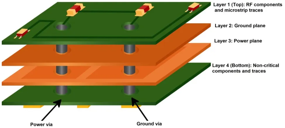
- Alternate Signal and Plane Layers: Place signal layers next to ground or power planes to provide a return path for signals and reduce EMI. For example, in a 4-layer PCB, a common stackup is Signal-Ground-Power-Signal.
- Minimize Signal Layer Adjacency: Avoid placing two signal layers directly next to each other, as this increases crosstalk. If unavoidable, route traces perpendicularly on adjacent layers to minimize interference.
- Control Impedance: Use specific dielectric thicknesses and materials to achieve target impedance. For instance, a 50-ohm trace on a 1.6mm FR-4 board might require a trace width of 0.3mm and a dielectric height of 0.2mm between the signal layer and ground plane.
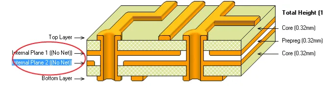
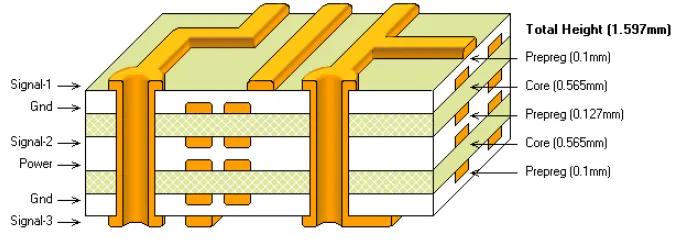
- Symmetry: Maintain a symmetrical stackup to prevent warping during manufacturing. For a 6-layer board, a balanced stackup might be Signal-Ground-Signal-Signal-Power-Signal.
Common Stackup Examples
Let’s look at typical stackups for different PCB complexities:
- 2-Layer PCB: Top (Signal), Bottom (Signal/Ground). Ideal for simple, low-cost designs but offers limited signal integrity.
- 4-Layer PCB: Top (Signal), Inner 1 (Ground), Inner 2 (Power), Bottom (Signal). A popular choice for moderate complexity, providing better EMI control.
- 6-Layer PCB: Top (Signal), Inner 1 (Ground), Inner 2 (Signal), Inner 3 (Signal), Inner 4 (Power), Bottom (Signal). Suitable for high-speed designs with multiple signal layers.
PCB Signal Layer Basics: Best Practices for Design
Now that we’ve covered the fundamentals of signal layers and stackups, let’s explore practical tips to optimize your PCB designs. These best practices will help you avoid common pitfalls and ensure reliable performance.
1. Route High-Speed Signals First
Always prioritize routing high-speed signals on inner layers near ground planes. This reduces exposure to external noise and ensures a consistent return path. For example, a 2.5 GHz signal might require a trace length matched to within 0.5mm to avoid timing issues in differential pairs.
2. Maintain Consistent Trace Widths
Keep trace widths uniform to avoid impedance mismatches. A sudden change from a 0.2mm to a 0.5mm trace can cause signal reflections, degrading performance. Use impedance calculators to determine the correct width based on your dielectric material and layer spacing.
3. Avoid Vias Where Possible
Vias introduce inductance and can disrupt high-speed signals. If vias are necessary, place them strategically and use back-drilling for high-frequency designs to remove unused via stubs, which can act as antennas for noise.
4. Use Ground Planes Effectively
A solid ground plane adjacent to a signal layer reduces loop area and improves signal return paths. Ensure there are no splits in the ground plane under high-speed traces, as this can increase inductance and EMI by up to 15-20% in some scenarios.
5. Test and Simulate Your Design
Before manufacturing, use simulation tools to analyze signal integrity. Tools can predict issues like crosstalk or signal delay, allowing you to tweak layer stackups or trace routing. For instance, a simulation might reveal that a 1ns delay in a critical signal path needs adjustment in trace length or layer placement.
Challenges in Managing Signal Layers and How to Overcome Them
Designing with signal layers isn’t without challenges. Here are some common issues and solutions to help you navigate them.
Challenge 1: Crosstalk Between Signal Layers
When signal layers are too close or improperly shielded, crosstalk can occur, leading to data errors. To mitigate this, increase spacing between traces (e.g., maintain at least 3x the trace width as spacing) and ensure a ground plane separates adjacent signal layers.
Challenge 2: Signal Loss in High-Speed Designs
At high frequencies, signal loss due to dielectric absorption or skin effect becomes significant. Use low-loss materials with a dielectric constant (Dk) below 3.5 and a loss tangent below 0.005 for frequencies above 1 GHz. Additionally, keep trace lengths as short as possible.
Challenge 3: Manufacturing Constraints
Complex stackups with many signal layers can increase manufacturing costs and lead times. Work closely with your fabrication partner to balance performance needs with budget constraints. Opt for standard layer counts (e.g., 4 or 6 layers) when possible to keep costs down.
Advanced Tips for Signal Layer Optimization
For experienced designers looking to push their designs further, consider these advanced strategies:
- Differential Pair Routing: For high-speed interfaces like USB 3.0, route differential pairs with equal lengths (matched to within 0.1mm) on the same signal layer to maintain signal timing.
- Controlled Dielectric Materials: Select materials like Rogers or Isola for high-frequency designs, as they offer tighter control over Dk (e.g., 3.0 ± 0.05) compared to standard FR4.
- Layer-Specific EMI Shielding: In ultra-sensitive designs, dedicate an entire layer to EMI shielding by surrounding critical signal layers with ground planes on both sides.
Conclusion: Mastering Signal Layers for Better PCB Designs
Signal layers are the backbone of any PCB, ensuring that electrical signals travel efficiently and without interference. By understanding signal layers, from their basic definition to the intricacies of stackup design, you can create PCBs that meet the demands of modern electronics. Remember the key takeaways: prioritize high-speed signals on inner layers, maintain controlled impedance, and always simulate your design before production.
Whether you’re working on a simple 2-layer board or a complex multilayer design, applying these PCB signal layer basics will elevate your skills as a designer. With careful planning and attention to detail, you can tackle challenges like crosstalk and signal loss, ensuring your projects succeed every time. Keep these principles in mind, and your next PCB design will be a step closer to perfection.


