ALLPCB


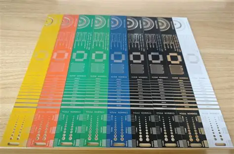
In the fast-evolving world of Internet of Things (IoT) devices, designing a printed circuit board (PCB) that balances size, cost, and performance is a critical challenge. An 8-layer PCB offers a powerful solution for IoT applications, providing the complexity needed for advanced functionality while allowing for compact designs. In this comprehensive guide, we’ll explore how 8-layer PCB design can be optimized for IoT devices, focusing on low-power consumption, compact layouts, cost efficiency, and seamless wireless connectivity.
Whether you’re an engineer working on smart home devices, wearable tech, or industrial IoT sensors, this blog will provide actionable insights into 8-layer PCB IoT applications, 8-layer PCB low-power design, 8-layer PCB compact design, 8-layer PCB cost optimization for IoT, and 8-layer PCB wireless connectivity. Let’s dive into the details of crafting high-performing IoT solutions with 8-layer PCBs.
Why Choose an 8-Layer PCB for IoT Devices?
IoT devices often require intricate designs to handle multiple components like sensors, microcontrollers, and wireless modules in a small footprint. An 8 layer PCB, with its multiple layers of conductive material separated by insulating layers, provides the necessary space for routing complex circuits while maintaining a compact size. Here’s why it’s an ideal choice:
- Increased Routing Density: With eight layers, you can route more signals in a smaller area, which is perfect for space-constrained IoT devices.
- Better Signal Integrity: Dedicated ground and power planes reduce noise and interference, ensuring reliable performance for high-speed data transfer in IoT applications.
- Support for Advanced Features: IoT devices often integrate wireless connectivity (like Wi-Fi or Bluetooth), requiring careful impedance control and shielding—achievable with an 8-layer structure.

Key Considerations for 8-Layer PCB IoT Applications
When designing an 8-layer PCB for IoT devices, several factors must be addressed to ensure the board meets the demands of modern applications. Let’s break down the critical aspects.
1. 8-Layer PCB Compact Design for Space Efficiency
IoT devices, such as smartwatches or environmental sensors, often need to fit into tiny enclosures. An 8-layer PCB compact design allows engineers to stack components and traces vertically across multiple layers, reducing the overall board size. Here are some tips for achieving compactness:
- Use High-Density Interconnect (HDI) Technology: HDI enables smaller vias (microvias) and finer traces, allowing more components to fit in a limited space. For example, trace widths as small as 3 mils (0.003 inches) can be achieved with HDI.
- Optimize Component Placement: Place high-speed components closer to their respective connectors to minimize trace lengths, reducing both size and signal delays.
- Leverage Both Sides: Utilize both the top and bottom layers for component placement to maximize space usage.
By focusing on a compact layout, you can design IoT devices that are not only smaller but also lighter, which is crucial for wearables and portable gadgets.

2. 8-Layer PCB Low-Power Design for Energy Efficiency
Energy efficiency is a top priority for IoT devices, many of which operate on battery power. An 8-layer PCB low-power design can significantly extend battery life. Here’s how to achieve it:
- Dedicated Power Planes: Use separate layers for power distribution to minimize voltage drops and ensure stable power delivery to low-power components. A typical power plane might maintain a voltage tolerance of ±5% for consistent performance.
- Reduce Parasitic Capacitance: Keep traces short and avoid unnecessary overlaps between layers to lower power loss due to capacitance.
- Integrate Power-Saving Components: Choose microcontrollers and sensors with sleep modes or low-power states, and design the PCB to support these features with minimal current leakage.
For instance, in a smart sensor node, optimizing the power plane design on an 8-layer PCB can reduce quiescent current draw to as low as 1 μA during sleep mode, extending battery life from months to years.
3. 8-Layer PCB Wireless Connectivity for Seamless Communication
Wireless communication is at the heart of IoT, whether it’s Wi-Fi, Bluetooth, Zigbee, or cellular connectivity. Designing an 8-layer PCB with effective 8-layer PCB wireless connectivity ensures reliable data transmission. Consider these strategies:
- Impedance Matching: Maintain controlled impedance for RF traces (typically 50 ohms for most wireless protocols) by using dedicated signal layers and ground planes to avoid signal loss.
- Shielding and Isolation: Use inner layers as ground planes to shield sensitive RF signals from interference caused by nearby digital circuits.
- Antenna Placement: Position antennas away from noisy components and ensure a clear ground plane beneath them for optimal radiation patterns. For a 2.4 GHz Bluetooth module, a clear area of at least 10 mm around the antenna is often recommended.
By prioritizing these design elements, you can achieve stable wireless performance, even in environments with high electromagnetic interference (EMI).

4. 8-Layer PCB Cost Optimization for IoT Projects
While 8-layer PCBs offer numerous advantages, they can be more expensive than simpler designs due to the increased number of layers and manufacturing complexity. However, 8-layer PCB cost optimization for IoT is possible with careful planning:
- Minimize Layer Usage: Only use all eight layers if necessary. For less complex IoT devices, reserve unused layers for future scalability rather than filling them with unnecessary traces.
- Standardize Materials: Opt for standard FR-4 material instead of high-frequency laminates unless your design requires specific dielectric properties. FR-4 typically costs 20-30% less than specialized materials.
- Optimize Manufacturing Parameters: Stick to standard board thicknesses (e.g., 1.6 mm) and avoid overly tight tolerances unless critical, as tighter specs can increase production costs by up to 50%.
Balancing functionality with cost is key. For example, a smart home IoT device might not need advanced materials if it operates at lower frequencies, saving significant costs without sacrificing performance.
Challenges in 8-Layer PCB Design for IoT and How to Overcome Them
Designing an 8-layer PCB for IoT applications comes with unique challenges. Below, we address common hurdles and provide practical solutions.
Challenge 1: Managing Heat Dissipation in Compact Designs
With components packed closely together on a small board, heat buildup can degrade performance or damage parts. To manage this:
- Use thermal vias to transfer heat from hot components to a dedicated ground plane for dissipation.
- Place heat-generating components, like power regulators, near the board edges for better airflow.
Challenge 2: Ensuring Signal Integrity at High Speeds
IoT devices often process high-speed signals for data transfer. Signal integrity issues, such as crosstalk, can arise if not addressed:
- Route high-speed signals on internal layers sandwiched between ground planes to reduce EMI.
- Maintain consistent trace widths and spacing. For a 5 GHz signal, a trace width of 6 mils with 10-mil spacing often works well to minimize crosstalk.
Challenge 3: Balancing Cost with Performance Needs
As mentioned earlier, cost can be a barrier. Beyond material and manufacturing choices, consider iterative prototyping to test designs before full-scale production. This approach can save costs by identifying issues early.
Best Practices for Designing an 8-Layer PCB for IoT Devices
To wrap up, here are some best practices to ensure your 8-layer PCB design meets the needs of modern IoT applications while balancing size, cost, and performance:
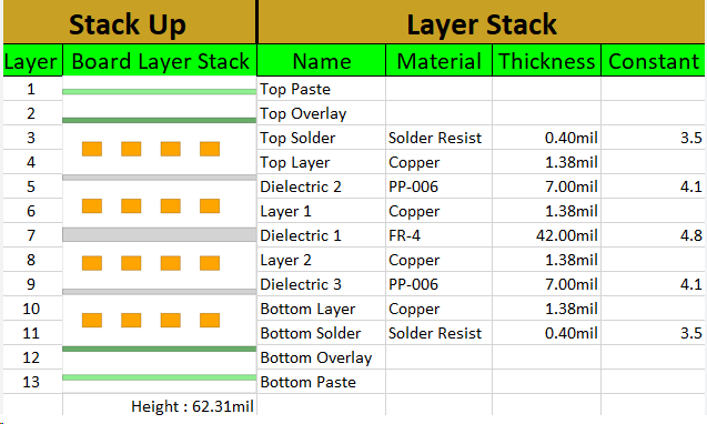
- Start with a Clear Stack-Up Plan: Define the purpose of each layer (e.g., signal, power, ground) early in the design process to avoid rework. A common stack-up might include two signal layers on top and bottom, with inner layers for power and ground.
- Simulate Before Building: Use simulation tools to test signal integrity, thermal performance, and power distribution before manufacturing.
- Prioritize Scalability: Design with future upgrades in mind. Leave room for additional components or features on unused layers.
- Collaborate with Manufacturers: Work closely with your PCB fabrication team to understand their capabilities and constraints, ensuring your design aligns with cost-effective production methods.
Conclusion: Mastering 8-Layer PCB Design for IoT Success
An 8-layer PCB offers a robust platform for creating advanced IoT devices that meet the demands of compactness, efficiency, and connectivity. By focusing on 8-layer PCB compact design, 8-layer PCB low-power design, and 8-layer PCB wireless connectivity, you can build devices that perform reliably in real-world conditions. Additionally, through careful 8-layer PCB cost optimization for IoT, it’s possible to keep expenses in check without compromising quality.
The journey of designing an 8-layer PCB for 8-layer PCB IoT applications involves understanding the unique requirements of your project and applying the strategies discussed in this guide. With the right approach, you can achieve a perfect balance of size, cost, and performance, paving the way for innovative IoT solutions that stand out in today’s competitive market.