 ALLPCB


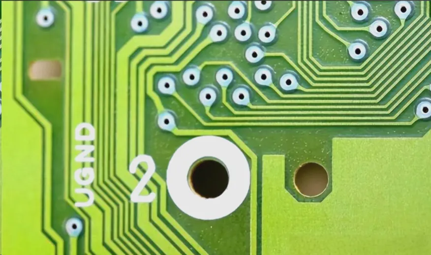
Grounding is a cornerstone of printed circuit board (PCB) design, directly impacting signal integrity, noise reduction, and overall performance. If you're searching for effective PCB grounding techniques, including methods like single point grounding PCB, star grounding PCB, and ground plane design PCB, you're in the right place. In this comprehensive guide, we'll dive deep into the art of grounding, offering practical tips and detailed insights to help you design robust and reliable PCBs.
Whether you're a seasoned engineer or just starting out, grounding can make or break your circuit's performance. Poor grounding often leads to issues like electromagnetic interference (EMI), signal crosstalk, or even complete system failure. By mastering the techniques discussed here, you'll be equipped to tackle these challenges head-on. Let's explore the essential strategies for grounding in PCB layout design.
Why Grounding Matters in PCB Design
Grounding serves as the foundation for any PCB, acting as a reference point for all signals and providing a return path for currents. Without proper grounding, high-frequency signals can interfere with each other, power supplies can become unstable, and noise can degrade performance. For instance, in high-speed designs, improper grounding might result in signal delays or data corruption, with studies showing that EMI can increase by up to 30% without optimized ground paths.
Effective grounding minimizes these risks by reducing loop areas, controlling impedance, and ensuring stable voltage levels. It's especially critical in mixed-signal designs, where analog and digital components share the same board. With this in mind, let’s break down the key PCB grounding techniques that can elevate your design.
Key PCB Grounding Techniques for Optimal Performance
Grounding isn't a one-size-fits-all solution. Different designs and applications call for specific approaches. Below, we’ll cover some of the most effective PCB grounding techniques, including single point grounding PCB, star grounding PCB, and ground plane design PCB, with actionable advice for implementation.
1. Single Point Grounding PCB: Minimizing Ground Loops
Single point grounding PCB is a technique where all ground connections converge at a single point. This method is particularly useful in low-frequency or analog circuits where ground loops can introduce noise. By connecting all ground paths to one central node, you prevent multiple return paths that could create loops and pick up unwanted interference.
For example, in an audio amplifier circuit, using single point grounding can reduce hum and buzz caused by ground loops. To implement this, identify a central ground point near the power supply input and route all ground connections directly to it. Be mindful of trace lengths—long traces can act as antennas, picking up noise. Aim to keep ground traces under 0.5 inches where possible to maintain low impedance, typically below 0.1 ohms at low frequencies.
However, single point grounding isn't ideal for high-frequency designs, as it can lead to high impedance at the grounding point. For such cases, other methods like ground planes are more effective.
2. Star Grounding PCB: Separating Analog and Digital Grounds
Star grounding PCB builds on the concept of single point grounding but takes it a step further by organizing ground connections in a star-like pattern. This technique is ideal for mixed-signal designs where analog and digital components coexist. The goal is to keep noisy digital grounds separate from sensitive analog grounds, connecting them only at a single point to avoid interference.
In practice, you might design a PCB for a microcontroller with analog sensors. Route the digital ground connections (from the microcontroller and digital ICs) to one branch of the star, and the analog ground connections (from sensors and amplifiers) to another. Both branches meet at a central ground point, often near the power supply or a ground plane connection. This setup can reduce noise coupling by up to 20 dB in sensitive circuits, ensuring cleaner signals for analog components.
Keep in mind that star grounding requires careful planning during the layout phase. Misplaced connections or long traces can negate the benefits, so use short, direct paths and consider splitting ground planes if needed.
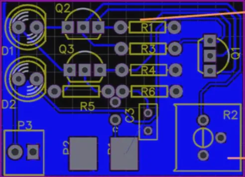
3. Ground Plane Design PCB: The Backbone of High-Speed Designs
When it comes to high-frequency or high-speed digital circuits, ground plane design PCB is often the go-to solution. A ground plane is a large, continuous layer of copper on the PCB dedicated to grounding. It provides a low-impedance return path for currents, reduces EMI, and stabilizes voltage levels across the board.
For instance, in a 5G communication module operating at frequencies above 1 GHz, a solid ground plane can minimize signal reflections and crosstalk. To design an effective ground plane, dedicate an entire layer (or multiple layers in multilayer boards) to grounding. Ensure the plane is unbroken as much as possible—avoid splitting it unnecessarily, as cuts can increase loop inductance and create noise. If splits are unavoidable, use stitching vias to connect ground planes across layers, maintaining a low-impedance path (ideally below 0.05 ohms).
Additionally, place decoupling capacitors close to power pins of ICs, connecting them directly to the ground plane. This reduces power supply noise, with typical capacitor values ranging from 0.1 μF to 1 μF for most digital circuits. A well-designed ground plane can improve signal integrity by up to 40% in high-speed applications.
Best Practices for Implementing PCB Grounding Techniques
While the techniques above provide a strong foundation, successful grounding requires attention to detail during the design and layout process. Here are some best practices to ensure your grounding strategy is effective across different applications.
Keep Ground Paths Short and Direct
Long ground traces increase impedance and can act as antennas, picking up or radiating noise. Always route ground connections as short and direct as possible. For high-speed signals (above 100 MHz), the return path should ideally be within 0.1 inches of the signal trace to minimize loop area and inductance.
Avoid Ground Loops at All Costs
Ground loops occur when multiple ground paths create a closed loop, allowing currents to flow unpredictably and introduce noise. Stick to single point or star grounding in low-frequency designs, and use solid ground planes for high-frequency boards to eliminate loops. If a loop is unavoidable, consider using a small resistor (e.g., 10 ohms) to break the loop without disrupting functionality.
Use Multiple Ground Vias for Multilayer Boards
In multilayer PCBs, connect ground planes across layers using multiple vias. This technique, known as via stitching, ensures a consistent low-impedance ground path. Space vias at intervals of about 0.2 inches along the board edges or near high-current areas to maintain uniformity. This can reduce ground bounce by up to 15% in dense designs.
Separate Analog and Digital Grounds Where Necessary
In mixed-signal designs, always isolate analog and digital grounds to prevent noise from digital switching (often at 1-10 MHz) from affecting analog signals. Use star grounding or split ground planes, connecting them at a single point near the power entry to maintain a common reference.
Common Grounding Mistakes to Avoid
Even with the best intentions, grounding errors can creep into PCB designs. Here are some common pitfalls and how to avoid them.
Splitting Ground Planes Incorrectly
While splitting ground planes can help isolate noisy and sensitive areas, doing so without proper planning can create high-impedance paths and increase EMI. If you must split, ensure the split is minimal and use capacitors or inductors to bridge the gap for high-frequency currents.
Ignoring Return Path Optimization
In high-speed designs, the return path for signals must follow the shortest route possible. If a signal trace crosses a split in the ground plane, the return current must detour, increasing loop area and noise. Always route signals over a continuous ground plane to maintain signal integrity.
Overlooking Decoupling Capacitors
Decoupling capacitors are critical for filtering noise from power supplies, yet they’re often placed too far from IC pins. Position these capacitors within 0.1 inches of the power pin, connecting them directly to the ground plane for maximum effectiveness.
Advanced Grounding Tips for Specific Applications
Different PCB applications demand tailored grounding strategies. Here’s how to adapt your approach for specific scenarios.
High-Speed Digital Circuits
For designs operating above 500 MHz, such as DDR memory or USB 3.0 interfaces, prioritize a solid ground plane on an adjacent layer to signal traces. Use impedance-controlled traces (typically 50 ohms for single-ended signals) and ensure return paths are uninterrupted. Adding guard traces connected to ground can further reduce crosstalk by up to 10 dB.
RF and Microwave Designs
In RF circuits, grounding affects impedance matching and signal loss. Use a ground plane with minimal vias or cuts to avoid parasitic inductance, which can shift resonant frequencies by 5-10%. Surround RF traces with ground vias spaced at 1/20th of the wavelength to create a Faraday cage effect, minimizing radiation.
Power Electronics
For high-current applications like motor drivers, focus on low-impedance ground paths to handle currents often exceeding 10 A. Use thick traces (at least 50 mils per ampere) or dedicated ground planes, and place high-current components close to the power source to reduce voltage drops.
Conclusion: Mastering the Art of Grounding
Grounding is both a science and an art in PCB design. By understanding and applying PCB grounding techniques like single point grounding PCB, star grounding PCB, and ground plane design PCB, you can significantly enhance the performance and reliability of your circuits. From minimizing noise with short ground paths to optimizing return currents with solid planes, each method offers unique benefits tailored to specific design needs.
Start by assessing the requirements of your project—whether it’s low-frequency analog, high-speed digital, or RF—and choose the grounding strategy that fits best. Combine this with best practices like via stitching and proper capacitor placement to build a robust foundation for your PCB. With these techniques in your toolkit, you’re well on your way to designing boards that perform flawlessly under any condition.


