ALLPCB


If you're new to PCB design and wondering how to make your boards easy to understand and assemble, PCB legend printing is a crucial skill to master. Often called silkscreen printing, this process involves adding text, symbols, and markings to your printed circuit board (PCB) for clear identification of components and connections. In this comprehensive guide, we'll walk you through the essentials of DIY PCB legend printing, offering a detailed PCB legend tutorial with tips for simple PCB legend design, easy PCB legend application, and a hobbyist PCB legend guide to help you get started.
Whether you're a hobbyist or an aspiring engineer, this blog will provide actionable advice to ensure your PCB markings are clear, professional, and functional. Let's dive into the world of PCB legend printing and explore how to achieve excellent results even as a beginner.
What Is PCB Legend Printing and Why Does It Matter?
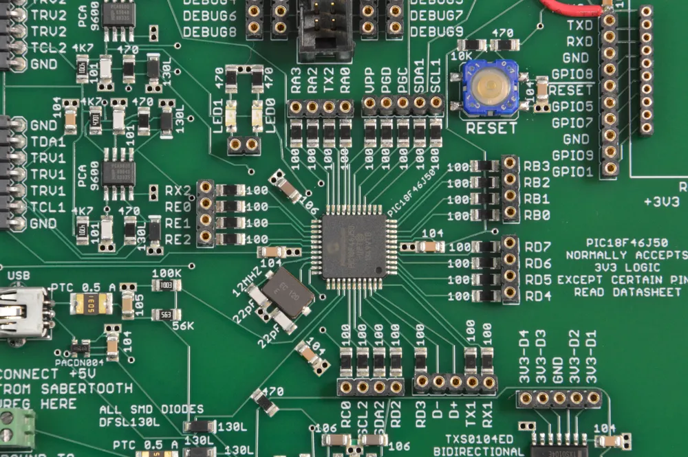
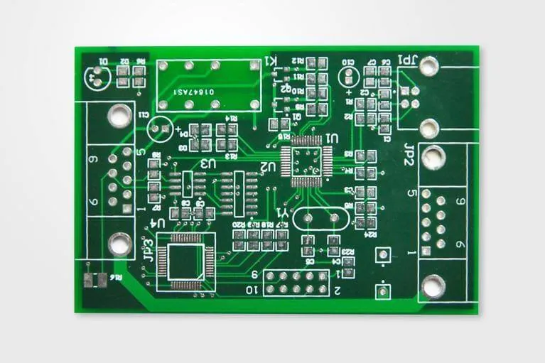
PCB legend printing, also known as silkscreen printing, is the process of adding informational text, symbols, and patterns to the surface of a printed circuit board. These markings typically include component reference designators (like R1 for a resistor or C2 for a capacitor), polarity indicators, test points, and other identifiers that guide assembly and troubleshooting.
For beginners, the importance of legend printing cannot be overstated. Without clear markings, assembling a PCB can become a guessing game, leading to errors like placing components in the wrong spots or soldering them incorrectly. A well-designed legend ensures that anyone working on the board—whether it's you or someone else—can quickly understand its layout and function. This is especially critical for hobbyists who may not have advanced tools or extensive experience.
Getting Started with DIY PCB Legend Printing: Tools and Materials
Before you begin, it's essential to gather the right tools and materials for DIY PCB legend printing. Here's a list of what you'll need as a beginner:
- PCB Design Software: Use a free or affordable design tool to create your legend layer. Popular options include software with user-friendly interfaces for hobbyists.
- Blank PCB or Prototype Board: Start with a simple single-layer or double-layer board for practice.
- Transfer Paper or Stencil (for DIY methods): If you're printing legends at home, transfer paper can help apply designs to the board.
- Printer: A standard inkjet or laser printer works for creating transfer designs.
- Silkscreen Ink or Paint Pen: For manual application, use a fine-tip paint pen or specialized silkscreen ink.
- Protective Gear: Gloves and a well-ventilated workspace are necessary if you're using chemicals or inks.
With these tools in hand, you're ready to start experimenting with legend printing on your PCB projects. For hobbyists on a budget, many of these items can be sourced affordably online or at local electronics stores.
Step-by-Step PCB Legend Tutorial for Beginners
Creating a clear and functional PCB legend doesn't have to be complicated. Follow this step-by-step PCB legend tutorial to achieve professional results, even if you're just starting out.
Step 1: Plan Your Legend Design
Before printing anything, plan what information your PCB legend needs to include. Focus on essential details like:
- Component reference designators (e.g., R1, C3).
- Polarity markings for diodes, capacitors, and LEDs.
- Pin numbers or connection points for ICs and connectors.
- Board name, version, or date for future reference.
Keep your design minimal to avoid clutter. A simple PCB legend design is often more effective than an overcrowded one. Use a design software to place these elements on the silkscreen layer, ensuring they don't overlap with solder pads or vias.
Step 2: Choose the Right Font and Size
Legibility is key in PCB legend printing. Select a clean, sans-serif font with a minimum height of 0.8 mm to 1 mm for text. Smaller text may not print clearly, especially with DIY methods. Most design software allows you to adjust font size and style, so test different options to find what works best for your board.
Step 3: Position Legends Strategically
Place text and symbols close to the components they describe, but avoid covering areas where soldering or mounting hardware will be. For example, position a resistor's label (like R1) next to its pads, and add an arrow or plus sign near a capacitor to indicate polarity. This strategic placement enhances usability during assembly and troubleshooting.
Step 4: Test Your Design Before Printing
Always preview your silkscreen layer in your design software to catch errors. Print a paper mockup of your PCB layout at a 1:1 scale and check if the text is readable and properly aligned. This step can save you from costly mistakes during the actual printing process.
Step 5: Apply the Legend to Your PCB
For easy PCB legend application, you have two main options as a hobbyist: professional manufacturing or DIY methods.
- Professional Manufacturing: If you're ordering your PCB from a fabrication service, upload your design files with the silkscreen layer included. Most services will handle legend printing with high precision using automated processes.
- DIY Method: For home projects, print your legend design onto transfer paper using a laser printer. Place the paper on your PCB, apply heat with an iron to transfer the design, and then carefully peel off the paper. Alternatively, use a fine-tip paint pen to manually draw markings if you're working on a small-scale project.
Step 6: Verify and Protect the Legend
After applying the legend, inspect it for clarity and accuracy. If you used a DIY method, ensure the ink or transfer has adhered properly without smudging. To protect the legend from wear during handling or soldering, consider applying a clear protective coating or solder mask over the silkscreen layer if your PCB design allows for it.
Essential Tips for Simple PCB Legend Design
Designing a simple PCB legend design is all about balancing functionality with aesthetics. Here are some beginner-friendly tips to keep in mind:
- Stick to Standard Colors: White ink on a green or blue solder mask is the most common and readable combination. Avoid colors that blend into the background.
- Use Consistent Orientation: Align text in the same direction (e.g., all horizontal) to make it easier to read at a glance.
- Avoid Overloading Information: Include only necessary details to prevent clutter. For small boards, prioritize critical markings over decorative elements.
- Account for Manufacturing Limits: If using a professional service, check their minimum line width and text size requirements for silkscreen printing. Typically, line widths below 0.15 mm may not print clearly.
By following these tips, you'll create a clean and effective legend that enhances your PCB's usability without overwhelming the design.
Common Mistakes to Avoid in Hobbyist PCB Legend Printing
As part of this hobbyist PCB legend guide, let's cover some pitfalls beginners often encounter and how to avoid them:
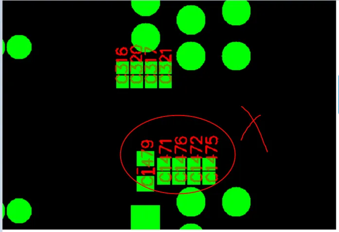
- Placing Text Over Pads or Vias: This can obscure important soldering areas and make assembly difficult. Always double-check your silkscreen layer for overlaps.
- Using Unreadable Fonts or Sizes: Tiny or overly stylized fonts can be hard to read, especially after printing. Stick to standard sizes and styles for clarity.
- Ignoring Polarity Markings: Forgetting to mark polarity for components like diodes or electrolytic capacitors can lead to assembly errors. Always include these indicators.
- Skipping the Preview Step: Not testing your design on paper or in software can result in misplaced or incorrect legends. Take the time to verify everything before finalizing.
Advanced Tricks for Better PCB Legend Printing
Once you've mastered the basics, try these advanced tricks to take your PCB legend printing to the next level:
- Use Alignment Marks: Add small crosshairs or alignment marks on your silkscreen layer to help with component placement during assembly, especially for surface-mount devices (SMDs).
- Incorporate Logos or Branding: If space allows, include a small logo or project name on the board for a professional touch. Keep it subtle to avoid clutter.
- Experiment with Layering: For complex boards, consider using both top and bottom silkscreen layers to distribute information evenly and reduce congestion on one side.
- Test Different Printing Methods: If DIY transfers don't yield the desired quality, explore stencil-based silkscreen printing for sharper results at home.
These tricks can add functionality and a polished look to your PCB, making it stand out even as a hobbyist project.
Why Clear Identification Matters for Hobbyists and Professionals Alike
Clear PCB legends are more than just labels—they're a roadmap for building and maintaining your electronics projects. For hobbyists, they simplify the learning process by reducing errors during assembly. For professionals, they ensure consistency and ease of collaboration when sharing designs with others. No matter your skill level, investing time in DIY PCB legend printing pays off in the form of more reliable and user-friendly boards.
Additionally, a well-marked PCB can save hours of troubleshooting. Imagine trying to debug a circuit without knowing which resistor is which or where a specific test point is located. A clear legend eliminates these headaches, making your projects more efficient from start to finish.
Conclusion: Start Printing Clear PCB Legends Today
Mastering PCB legend printing for beginners is an achievable goal with the right approach and tools. By following this PCB legend tutorial, focusing on simple PCB legend design, practicing easy PCB legend application, and using this hobbyist PCB legend guide, you can create boards that are easy to assemble and troubleshoot. Remember to plan your design carefully, use legible fonts and strategic placement, and avoid common mistakes that can compromise clarity.
Whether you're building a small prototype at home or preparing a design for professional fabrication, clear identification through legend printing is a skill worth developing. Start with a simple project, apply the tips and tricks shared in this guide, and watch as your PCB designs become more professional and functional. With practice, you'll gain confidence in creating legends that make your boards both practical and visually appealing.