 ALLPCB


Designing a rigid PCB layout can seem daunting, but with the right PCB design software and a step-by-step approach, you can create professional and functional boards for your electronics projects. Whether you're a beginner or an experienced engineer, this guide will walk you through the process of using popular tools like Altium Designer, KiCad, and Eagle for rigid PCB layout. We'll cover essential tips, tutorials, and best practices to help you master PCB design software and create high-quality layouts. Let's dive into the details of crafting a rigid PCB layout with confidence using these powerful tools.
What Is Rigid PCB Layout and Why Use Design Software?
A rigid PCB (Printed Circuit Board) is a solid, inflexible board used in most electronic devices to connect components through conductive tracks and pads. Designing a rigid PCB layout involves placing components and routing traces in a way that ensures functionality, reliability, and manufacturability. PCB design software simplifies this process by offering tools for schematic capture, component placement, trace routing, and design rule checking (DRC) to avoid errors.
Using software for rigid PCB layout saves time, reduces mistakes, and allows you to simulate and test your design before manufacturing. With features like 3D visualization and automated routing, these tools help ensure your board meets electrical and mechanical requirements. In this blog, we'll explore how to use three widely-used PCB design software options to create effective rigid PCB layouts.

Getting Started with PCB Design Software for Rigid Layouts
Before diving into specific tools, let's outline the general steps for designing a rigid PCB layout using any software. These steps apply across platforms and form the foundation of a successful design process:
- Create a Schematic: Start by drawing a schematic that defines how components are connected electrically.
- Component Placement: Place components on the board layout, considering factors like signal flow and heat dissipation.
- Routing Traces: Connect components with traces, ensuring minimal interference and proper impedance matching.
- Design Rule Check (DRC): Use software tools to check for errors like overlapping traces or incorrect clearances.
- Generate Output Files: Export Gerber files and other manufacturing data for production.
Now, let's explore how to apply these steps using three popular PCB design software tools, focusing on tutorials and tips for rigid PCB layouts.
Altium Designer Tutorial for Rigid PCB Layout
Altium Designer is a professional-grade PCB design software known for its advanced features and user-friendly interface. It’s ideal for complex rigid PCB layouts with high-speed signals or multilayer boards. Here's a step-by-step guide to using this tool for your rigid PCB design:
Step 1: Schematic Creation
In Altium Designer, start by creating a new project and adding a schematic sheet. Use the library panel to drag and drop components like resistors, capacitors, and ICs onto the sheet. Connect them with wires to define the circuit. For example, if you're designing a power supply board, ensure that high-current components are placed close to the input to minimize voltage drops.
Step 2: Board Layout and Component Placement
Once the schematic is complete, synchronize it with a new PCB layout file. Import the components and arrange them on the board. Pay attention to placement—group related components together to reduce trace lengths. For instance, place decoupling capacitors within 0.1 inches of IC power pins to reduce noise.
Step 3: Routing and Impedance Control
Use the interactive routing tool to draw traces between components. For high-speed designs, maintain controlled impedance by setting trace widths based on the board’s dielectric constant and layer stack-up. A typical 50-ohm impedance trace on a standard FR4 board might require a width of 6 mils on a 1 oz copper layer. Use the software’s calculator to verify this.
Step 4: Design Rule Check and Validation
Run a DRC to ensure your layout meets manufacturing and electrical standards. Check for minimum clearance (e.g., 8 mils between traces) and via sizes (e.g., 12 mil drill diameter for standard vias). Fix any errors before proceeding.
Step 5: Output Generation
Generate Gerber files, drill files, and a Bill of Materials (BOM) for manufacturing. Use the 3D view to inspect the board for mechanical fitment issues, ensuring components don’t interfere with enclosures.
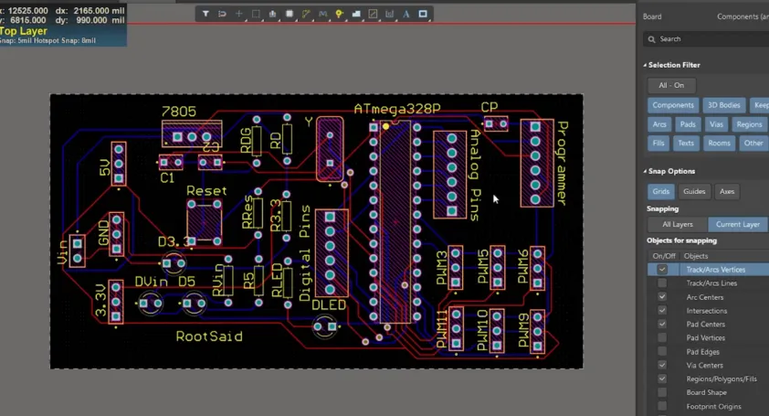
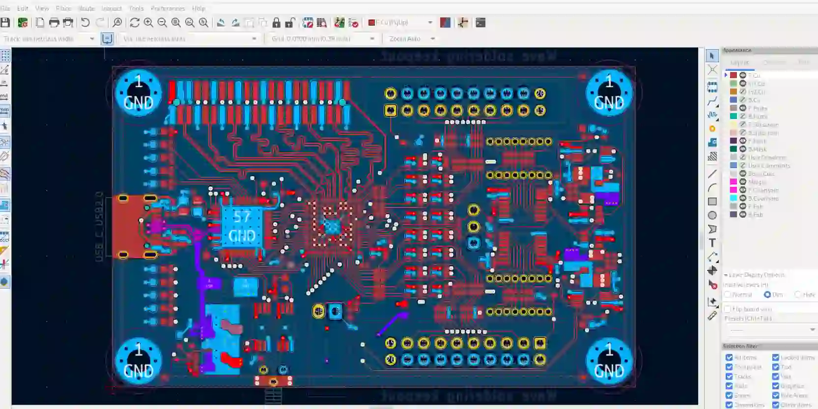
KiCad Tutorial for Rigid PCB Layout
KiCad is a free, open-source PCB design software that’s perfect for hobbyists and professionals looking for a cost-effective solution. It offers robust tools for rigid PCB layouts. Follow these steps to design your board with KiCad:
Step 1: Schematic Design in Eeschema
Start by launching Eeschema, KiCad’s schematic editor. Add components from the built-in libraries or create custom symbols if needed. Draw connections using the wire tool. For a simple LED circuit, ensure the resistor is in series with the LED to limit current to around 20 mA.
Step 2: Assign Footprints and Transfer to PCB Editor
Assign footprints to each component in the schematic (e.g., a 0805 footprint for a surface-mount resistor). Then, transfer the design to Pcbnew, KiCad’s layout editor, to start placing components on the board.
Step 3: Component Placement and Routing
Arrange components logically, keeping power and ground traces short to minimize noise. Use the routing tool to connect pads with traces. For a two-layer board, route high-priority signals on the top layer and use the bottom layer for ground planes to reduce electromagnetic interference (EMI).
Step 4: Define Design Rules and Check Errors
Set design rules like minimum trace width (e.g., 10 mils for low-current signals) and clearance (e.g., 8 mils). Run a DRC to catch issues like unconnected nets or overlapping traces. KiCad also offers a 3D viewer to visualize the final board.
Step 5: Export Manufacturing Files
Generate Gerber files and drill files using the plot tool. Ensure all layers (copper, silk screen, solder mask) are included for manufacturing.
Eagle PCB Design Tutorial for Rigid Layout
Eagle is another popular PCB design software, widely used for its simplicity and integration with various component libraries. It’s a great choice for small to medium-sized rigid PCB projects. Here’s how to use it:
Step 1: Create a Schematic
Open Eagle’s schematic editor and add components from the library. Connect them with nets to define the circuit. For example, in a microcontroller board, place the crystal oscillator close to the MCU pins to ensure stable clock signals at 16 MHz.
Step 2: Switch to Board Layout
Switch to the board editor to place components. Use the grid settings (e.g., 0.05-inch grid) for precise placement. Group related components to optimize trace routing and reduce signal delays.
Step 3: Route Traces Manually or Automatically
Use manual routing for critical signals or the autorouter for less complex designs. Ensure power traces are wider (e.g., 20 mils for 1A current) to handle higher currents without overheating. Add vias to switch layers when needed.
Step 4: Run Design Rule Checks
Configure DRC settings to match your manufacturer’s capabilities, such as minimum trace spacing of 6 mils. Run the check to identify and fix errors like unconnected pins or insufficient clearances.
Step 5: Prepare Files for Manufacturing
Use Eagle’s CAM processor to generate Gerber files and drill data. Review the output in a Gerber viewer to ensure all layers are correct before sending them for production.
Key Tips for Effective Rigid PCB Layout Across Software
Regardless of the software you choose, certain best practices apply to all rigid PCB layouts. These tips will help you create reliable and manufacturable designs:
- Plan Your Layer Stack-Up: For multilayer boards, define your stack-up early. A common 4-layer stack-up might include signal, ground, power, and signal layers. This helps with EMI reduction and signal integrity.
- Minimize Signal Crosstalk: Keep high-speed traces (e.g., signals above 100 MHz) away from each other or use ground planes to shield them. Maintain at least 3 times the trace width as spacing to avoid interference.
- Thermal Management: Place heat-generating components like voltage regulators away from sensitive parts. Add thermal vias (e.g., 0.3 mm diameter) under high-power components to dissipate heat to other layers.
- Test Points: Include test points for critical nets to facilitate debugging after manufacturing. Ensure they’re accessible and labeled clearly in the silkscreen layer.
- Documentation: Add clear silkscreen labels for component values and polarities. This helps during assembly and reduces errors.
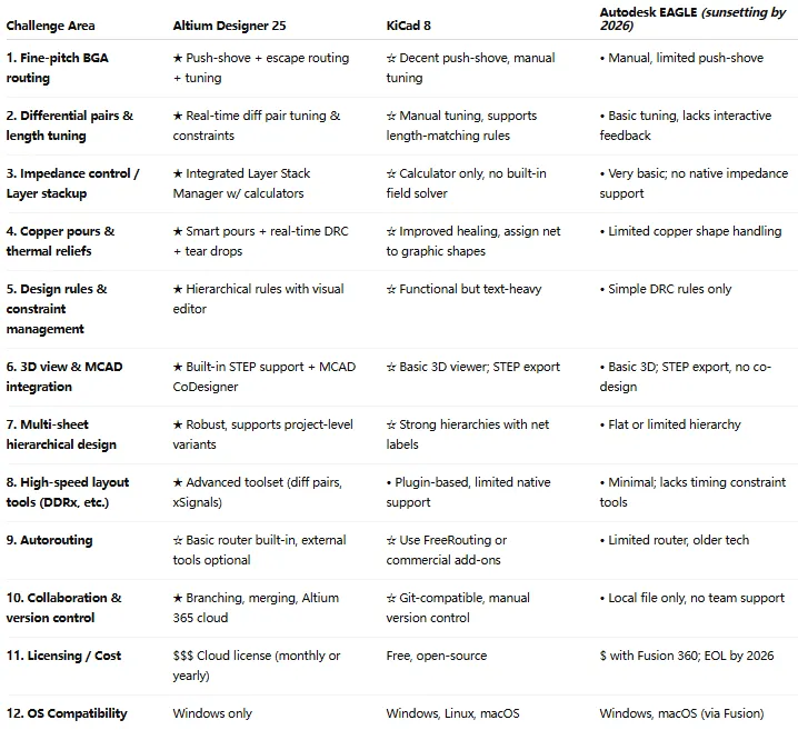
Choosing the Right PCB Design Software for Your Needs
Each software has its strengths for rigid PCB layouts. Here's a quick comparison to help you decide:
- Altium Designer: Best for professional, complex designs with high-speed requirements. It offers advanced simulation and 3D modeling but comes with a higher cost.
- KiCad: Ideal for budget-conscious users or open-source enthusiasts. It’s free and supports most rigid PCB design needs with a growing community for support.
- Eagle: Great for small to medium projects with an intuitive interface. It’s widely used by hobbyists and startups but may lack advanced features for very complex designs.
Consider your project’s complexity, budget, and learning curve when selecting a tool. All three can produce high-quality rigid PCB layouts with the right approach.
Common Challenges in Rigid PCB Layout and How to Overcome Them
Designing rigid PCBs comes with challenges, but PCB design software can help you address them:
- Signal Integrity Issues: High-speed signals can suffer from reflections if traces aren’t matched properly. Use software tools to calculate trace lengths and add termination resistors (e.g., 50 ohms) where needed.
- Component Density: Overcrowded boards lead to routing difficulties. Use smaller components (e.g., 0402 packages) or increase board size to create more space.
- Manufacturing Constraints: Not all designs are manufacturable due to tight tolerances. Stick to standard design rules like minimum trace width of 6 mils and via drill size of 10 mils to ensure compatibility with most fabricators.
Final Thoughts on Using PCB Design Software for Rigid Layouts
Mastering rigid PCB layout with PCB design software is a valuable skill for any electronics engineer. Whether you choose Altium Designer, KiCad, or Eagle, each tool offers unique features to help you create functional and reliable boards. By following the steps and tips outlined in this guide, you can tackle projects of varying complexity with confidence. Start with a clear schematic, plan your layout carefully, and use the software’s validation tools to ensure a manufacturable design. With practice, you’ll be able to optimize your rigid PCB layouts for performance and efficiency.
At ALLPCB, we’re committed to supporting your PCB design journey from concept to production. Use these tutorials and tips to refine your skills, and let us help you bring your designs to life with high-quality manufacturing services tailored to your needs.


