 ALLPCB


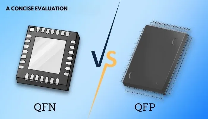
When designing a printed circuit board (PCB), selecting the right integrated circuit (IC) package can make or break your project. Two of the most popular surface-mount options—Quad Flat No-lead (QFN) and Quad Flat Package (QFP)—offer distinct advantages depending on your application. Whether you're optimizing for space, thermal performance, or ease of assembly, understanding the differences between QFN and QFP packages is critical for engineers aiming to balance performance, cost, and manufacturability.
In this blog, we'll dive into the specifics of QFN and QFP packages, compare their key features, and provide practical insights to help you choose the best option for your PCB design. From pin configurations to PCB thermal management, we've got you covered with actionable details to guide your decision-making process.
What Are QFN and QFP Packages?
Before we compare these two packages, let's define what they are and how they function in PCB design.
QFN Packages: Compact and Leadless
QFN stands for Quad Flat No-lead. As the name suggests, this package has no protruding leads. Instead, it features exposed metal pads (lands) on the bottom surface, which connect directly to the PCB via solder joints. A typical QFN package ranges from 2x2 mm to 12x12 mm in size, with pin counts often between 8 and 100. The exposed thermal pad on the underside enhances heat dissipation, making QFNs a go-to choice for compact, high-performance designs.
QFP Packages: Versatile and Leaded
QFP, or Quad Flat Package, is a surface-mount IC package with 'gull-wing' leads extending from all four sides. These leads provide electrical connections to the PCB and come in various pitches (e.g., 0.4 mm to 1.0 mm), supporting pin counts from 32 to over 200. QFP packages are larger than QFNs—often 7x7 mm to 20x20 mm or more—but their exposed leads make them easier to inspect and rework.
Key Differences Between QFN and QFP Packages
To choose the right package, you need to understand how QFN and QFP differ in design and performance. Let's break it down.
1. Lead Configuration
- QFN: No leads—electrical contacts are flat pads on the bottom. This leadless design reduces parasitic inductance (typically <1 nH per pin) and capacitance, improving signal integrity at high frequencies (e.g., >1 GHz).
- QFP: Features gull-wing leads extending outward. These leads increase inductance (around 2-5 nH per pin) due to their length, which can impact high-speed signals.
2. Size and Footprint
- QFN: Smaller and more compact, ideal for space-constrained designs. For example, a 32-pin QFN might occupy 5x5 mm, while a comparable QFP takes up 7x7 mm or more.
- QFP: Larger footprint due to the protruding leads, which can limit component density on the PCB.
3. Thermal Performance
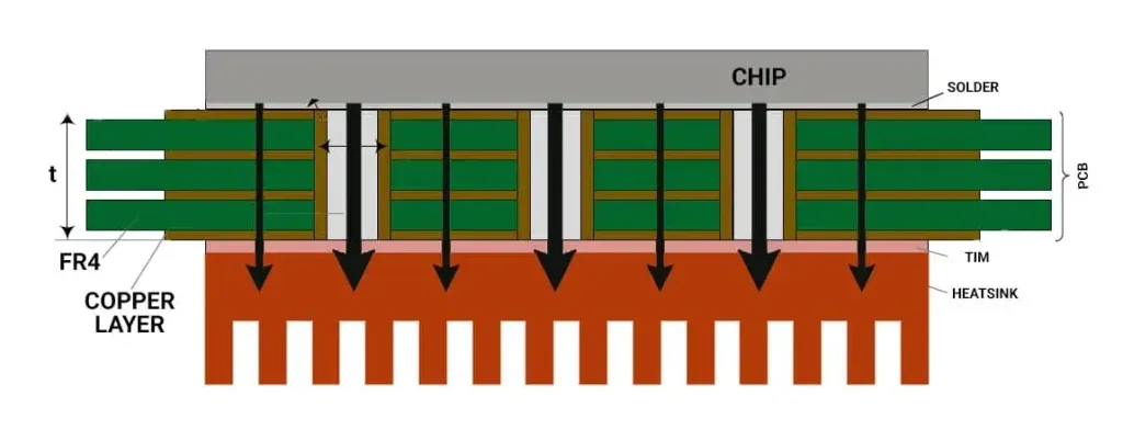
- QFN: Excels here thanks to the exposed thermal pad, which can reduce thermal resistance to as low as 10-15°C/W when soldered to a PCB with thermal vias. Perfect for power-hungry ICs like amplifiers or voltage regulators.
- QFP: Relies on leads and the package body for heat dissipation, with thermal resistance often exceeding 30°C/W unless enhanced with a heat sink.
4. Pin Count
- QFN: Typically supports fewer pins (up to 100), suitable for simpler ICs like sensors or small microcontrollers.
- QFP: Handles higher pin counts (up to 256 or more), making it a favorite for complex devices like microprocessors or FPGAs.
5. Assembly and Inspection
- QFN: Requires precise soldering (e.g., reflow with a stencil aperture of 0.25-0.3 mm) and X-ray inspection due to hidden solder joints. Rework is challenging.
- QFP: Easier to solder and inspect visually, thanks to exposed leads. Rework is straightforward with standard tools like a soldering iron.
Advantages and Disadvantages of QFN Packages
Advantages
- Space Efficiency: The small footprint saves valuable PCB real estate, critical for wearables or IoT devices.
- Superior Thermal Management: The thermal pad ensures efficient heat transfer, ideal for ICs dissipating 1-5 W.
- Electrical Performance: Low inductance and capacitance enhance performance in RF and high-speed applications (e.g., signal speeds >500 MHz).
- Cost-Effective for Small Designs: Fewer materials and simpler construction can lower costs in compact projects.
Disadvantages
- Assembly Complexity: Requires precise solder paste application and reflow profiles (e.g., peak temperature of 245-260°C) to avoid voids or misalignment.
- Inspection Challenges: Hidden joints demand X-ray equipment, increasing custom PCB cost by 10-20%.
- Limited Pin Count: Not suitable for ICs needing extensive I/O connections.
Advantages and Disadvantages of QFP Packages
Advantages
- High Pin Count: Supports complex ICs with 100+ connections, perfect for processors or telecom hardware.
- Ease of Assembly: Gull-wing leads self-align during reflow, reducing placement errors by up to 15% compared to QFN.
- Rework-Friendly: Exposed leads simplify repairs, cutting downtime in prototyping phases.
- Proven Reliability: Widely used for decades, with established manufacturing processes.
Disadvantages
- Larger Size: Takes up more space, a drawback in miniaturized designs.
- Thermal Limitations: Less efficient heat dissipation without additional cooling solutions.
- Signal Integrity: Higher inductance can degrade performance in high-frequency circuits (>1 GHz).
When to Choose QFN vs. QFP
Your choice depends on your project's priorities. Here's a practical guide based on common engineering scenarios.
Choose QFN When:
- Space Is Tight: If your PCB is <50 cm², QFN's compact size maximizes density.
- Heat Is a Concern: For ICs generating >2 W, the thermal pad keeps temperatures in check.
- High Speeds Matter: Applications like 5G modules or RF transceivers benefit from QFN's low parasitics.
- Example: A wearable fitness tracker with a 16-pin QFN sensor IC fits perfectly in a 3x3 mm footprint, dissipating 1.5 W efficiently.
Choose QFP When:
- Pin Count Is High: Complex ICs like a 144-pin microcontroller need QFP's capacity.
- Prototyping Is Key: Easier inspection and rework save time during development.
- Moderate Speeds Suffice: For signal speeds <500 MHz, QFP's inductance is manageable.
- Example: A 64-pin QFP in an industrial controller offers reliable connections and simple assembly for a 10x10 cm PCB.
Assembly Considerations for QFN and QFP
Both packages use surface-mount technology, but their assembly processes differ.
QFN Assembly Tips
- Solder Paste: Use a 0.1-0.15 mm thick stencil to apply paste evenly, avoiding excess that causes bridging.
- Reflow Profile: Maintain a peak temperature of 245-260°C for 20-40 seconds to ensure proper wetting without damaging the IC.
- Thermal Vias: Add 4-6 vias (0.3 mm diameter) under the thermal pad to reduce thermal resistance by 20-30%.
- Inspection: X-ray systems detect voids, targeting <15% voiding for automotive-grade reliability.
QFP Assembly Tips
- Lead Alignment: Use a pick-and-place machine with ±0.05 mm accuracy to position leads on pads.
- Reflow: A nitrogen atmosphere (O? <500 ppm) minimizes oxidation, ensuring joint strength.
- Visual Check: Confirm lead coplanarity (within 0.1 mm) to prevent open circuits.
- Rework: Desolder with a hot air gun at 300-350°C, keeping surrounding components safe.
Real-World Applications
QFN in Action
- Consumer Electronics: Smartphones use 32-pin QFNs for power management ICs, leveraging their 4x4 mm size and 2 W heat dissipation.
- Automotive: ADAS sensors in QFNs handle 1 GHz signals with minimal noise, thanks to low inductance.
QFP in Action
- Telecom: Base stations rely on 128-pin QFPs for DSP chips, supporting extensive I/O and easy maintenance.
- Industrial: PLCs with 100-pin QFPs offer robust connections for factory automation systems.
How ALLPCB Supports Your QFN and QFP Projects
When bringing your QFN or QFP-based PCB to life, partnering with the right manufacturer is key. At ALLPCB, we offer quick-turn prototyping to test your designs in as little as 24 hours, ensuring you can iterate fast—especially critical for QFP's rework-friendly nature. Our advanced manufacturing capabilities handle QFN's precise soldering needs, with X-ray inspection to guarantee joint quality. Plus, our global logistics network delivers your boards anywhere, fast, so you can meet tight deadlines without compromising on quality.
Conclusion: Making the Right Choice
Choosing between QFN and QFP packages comes down to your project's needs. If you prioritize space, thermal efficiency, and high-speed performance, QFN is your pick. If you need high pin counts, ease of assembly, and rework flexibility, QFP shines. By weighing factors like size, heat, and signal requirements—backed by the data we've shared—you can confidently select the right IC package for your PCB.
Ready to design your next board? Evaluate your specs, test both options if needed, and let us help you turn your vision into reality with precision and speed.


