 ALLPCB


1. Basic MOSFET Knowledge
MOS is short for MOSFET, metal-oxide semiconductor field-effect transistor. MOSFETs are classified as enhancement-mode and depletion-mode. An enhancement-mode device is normally off at VGS = 0; applying a proper VGS attracts carriers to the gate region and “enhances” channel conductivity. A depletion-mode device is fabricated with dopants that induce a channel at VGS = 0; it can be controlled with positive, zero, or negative gate voltages.
Enhancement-mode MOSFETs are commonly used in switching and high-power applications, while some amplifier or RF circuits may use depletion-mode devices. This article uses enhancement-mode MOSFETs as examples to explain device characteristics and practical failure cases.
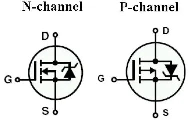
1.1 Enhancement NMOS
An NMOS conducts when VGS > VGS(th) and is suitable for source-to-ground low-side switching. VGS(th) values (for example 4 V, 10 V) are set by process and should be checked in the device datasheet.
1.2 Enhancement PMOS
A PMOS conducts when VGS is below a certain (negative) threshold and is suitable for source-to-positive-supply high-side switching. PMOS devices are convenient for high-side use but typically have higher RDS(on), higher cost, and fewer drop-in replacements; therefore many designs prefer NMOS devices when possible.
2. Key MOSFET Parameters
2.1 VDS
Select a MOSFET with a VDS rating higher than the maximum drain-to-source voltage expected in operation to avoid breakdown. Higher voltage ratings generally increase device cost.
2.2 VGS
VGS is the gate-to-source voltage rating. For the same device, VGS is usually lower than VDS. In practice, a transient voltage suppressor or zener is often connected across G and S to limit VGS.
2.3 VGS(th)
VGS(th) is the gate threshold where the MOSFET begins to conduct. For an NMOS, when 0 < VGS < VGS(th) the device is in a weakly conductive region with a depletion layer; only when VGS > VGS(th) does a channel form and the drain-source path conduct strongly.
2.4 ID
ID is the maximum continuous drain current the device can handle. Exceeding this current causes irreversible physical damage.
2.5 RDS(on)
RDS(on) is the on-state resistance between D and S under specified VGS, junction temperature, and ID. It determines conduction losses and heating. RDS(on) decreases with higher VGS and increases with higher junction temperature. Incorrect selection can lead to device failure under heavy load.
2.6 Junction Temperature
Junction temperature is the actual internal device temperature and is normally higher than the package surface temperature. The difference equals the thermal resistance RθJC (in °C/W) times the dissipated power. A common approximation is: junction temperature ≈ RθJC * power + ambient temperature. Maximum junction temperatures are typically in the 150–175 °C range; consult the datasheet for exact limits.
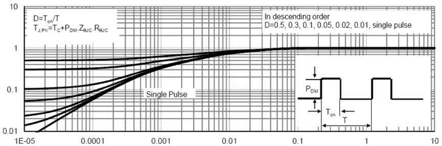
2.7 Thermal Resistance and Transient Factors
RθJC depends on package and process. For transient heating, RθJC is multiplied by a time-dependent factor: 1 for steady-state heating, and <1 for pulsed events. The factor varies by device; consult the transient thermal response curves in the datasheet.
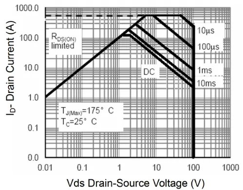
2.8 SOA (Safe Operating Area)
The SOA defines the safe combinations of voltage and current for which the device can operate without damage. For power MOSFETs the SOA depends on maximum single-pulse current IDmax, maximum VDS, maximum allowable power Pmax, and pulse duration t. Operating outside the SOA risks device failure.
3. Case Study 1
3.1 Problem Description
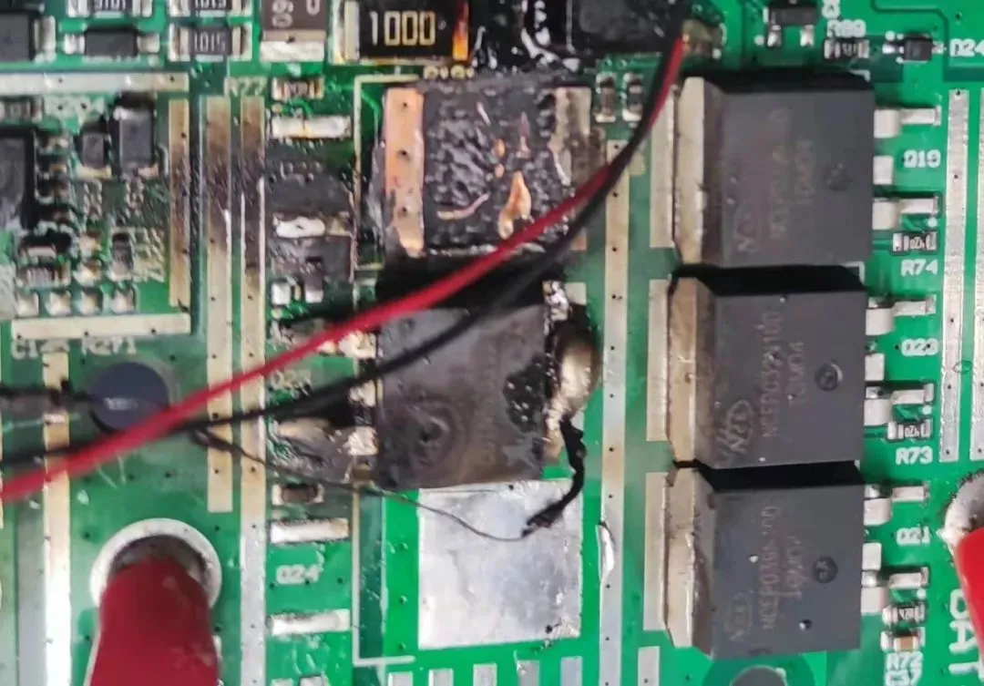
On a battery protection board, during a high-current discharge down to below the undervoltage threshold, the protection logic should turn the MOSFETs off. However, the MOSFETs remained conducting. Possible causes were a software bug preventing turn-off, or a MOSFET failure presenting as a short circuit that software could not overcome.
3.2 Root-Cause Analysis
Disassembling the battery pack revealed one discharge MOSFET running hot (the discharge path used four parallel MOSFETs). The insulation pad below this MOSFET was deformed by heat, strongly suggesting MOSFET failure. Removing that MOSFET and measuring with a multimeter showed a D-S short; the other parallel MOSFETs were normal, indicating a single-device failure.
3.3 Reproduction
Replacing the failed MOSFET with a new device from a different material lot (different silk-screen marking) and repeating the high-current discharge to undervoltage caused the MOSFET at that same position to fail again. Repeating the test consistently reproduced the failure, and it was always the newly replaced device that failed, regardless of position.
When all four parallel MOSFETs were replaced with devices from the same lot, the issue disappeared.
3.4 Analysis
The behavior suggests parameter mismatch between paralleled MOSFETs. One device may conduct first or have much lower on-resistance, taking the majority of transient current and failing. However, oscilloscope measurements of VGS showed a gate glitch prior to the intended turn-on: a small pulse of about 5 V (normal full conduction requires VGS > 10 V). The MOSFET was therefore in a half-on state. In this partially-on state the device has high RDS(on) while the external condition imposed large current, making the MOSFET vulnerable to breakdown.
Using a mix of three original MOSFETs plus one new MOSFET and monitoring the discharge MOSFET output voltage from the host showed that the glitch occurred before the software-issued turn-on. The MOSFET was damaged during the interval between the glitch and the intended software gate drive.
3.5 Mitigation
Further investigation showed the gate control was being disturbed by a hardware pin-check sequence that briefly pulled a pin to ground before software enabled the MOSFET. That sequence interfered with the gate level and produced a half-on condition during high-current discharge, leading to MOSFET failure.
Lessons from this case:
- Paralleled MOSFETs should be matched from the same production lot to avoid parameter mismatches that concentrate current in a single device.
- If VGS does not fully establish a low-RDS(on) state before high current flows, the MOSFET can overheat and fail due to excessive conduction losses.
4. Case Study 2
4.1 Problem Description
On another battery protection board, MOSFETs smoked and were destroyed during short-circuit testing. The failure was reproducible across multiple boards.
4.2 Root-Cause Hypothesis
Theoretical causes for short-circuit-driven MOSFET failure include hardware defects, incorrect component selection, or junction overheating leading to breakdown. Testing pointed to a hardware/material issue that caused the junction temperature to exceed limits. Replacing the MOSFET with a higher-performance device or shortening the MOSFET turn-off time eliminated the failure. The following sections present waveform observations and theoretical calculations supporting this conclusion.
4.3 Reproduction and Waveforms
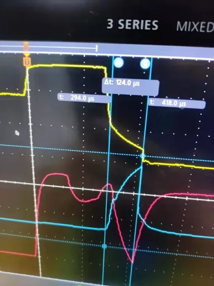
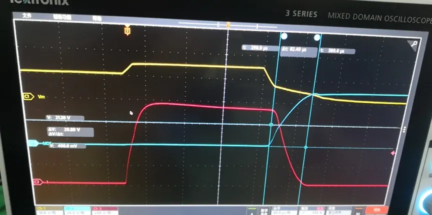
Two test setups were prepared: one where the MOSFET failed and one where it survived. Oscilloscope captures recorded VDS, VGS and ID. (Yellow: VGS, Blue: VDS, Red: ID.)
Figure 5 shows the failure waveform. After the short circuit occurs the controller issues a turn-off command and the current (red) starts to decrease, but near the end the MOSFET is punched through and current rapidly rises again.
Figure 6 shows a non-failure waveform for a modified circuit that reduced the MOSFET turn-off time from 124 us to 82.4 us; with the shorter turn-off the MOSFET no longer failed.
4.4 Theoretical Analysis 1
Test conditions: pack voltage = 56 V; single-MOS instantaneous peak current at short = 234 A; MOS turn-off interval = 124 us.
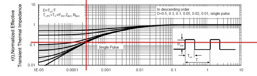
During the turn-off interval the current falls from peak to zero while VDS rises from zero to the full voltage. The instantaneous power waveform resembles the product of two linear ramps. The analysis approximates a maximum effective power Pmax = 0.5*Vmax * 0.5*Imax. For safety margin, the calculation assumes the dissipated power equals this Pmax throughout the interval.
Using the device SOA chart, select a representative point at 28 V and 117 A; the intersection corresponds to approximately 100 us. Under the assumed power level P = 0.5*56 V * 0.5*234 A, the MOSFET can only safely withstand about 100 us. This explains why a 124 us turn-off allowed damage while an 80 us turn-off did not.
4.5 Theoretical Analysis 2: Junction Temperature
Examining junction heating provides further insight into why the SOA limit is exceeded. The MOSFET datasheet lists RθJC = 0.68 °C/W.
Measured durations: short-circuit pulse 255 us; turn-off intervals of interest: 120 us and 80 us.
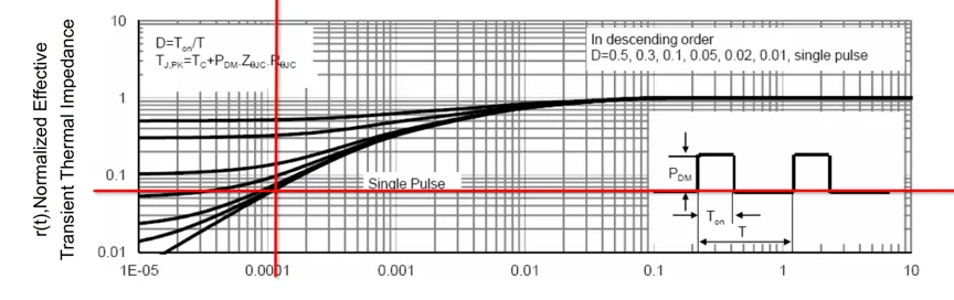
From the device transient thermal curves, the thermal factors are approximately:
- 255 us pulse: factor ≈ 0.14 → effective thermal resistance = 0.14 * 0.68 = 0.0952 °C/W
- 120 us turn-off: factor ≈ 0.06 → effective thermal resistance = 0.06 * 0.68 = 0.0408 °C/W
- 80 us turn-off: factor ≈ 0.045 → effective thermal resistance = 0.045 * 0.68 = 0.0306 °C/W
Temperature rise due to the short 255 us pulse (I^2R heating):
DeltaT_short = 0.0952 °C/W * I^2 * R = 0.0952 * 234^2 * 0.0035 ≈ 18.24 °C
Temperature rise during 120 us turn-off (power-based):
DeltaT_120 = 0.0408 °C/W * Pmax = 0.0408 * (56 V / 2 * 234 A / 2) ≈ 133.28 °C
Temperature rise during 80 us turn-off:
DeltaT_80 = 0.0306 * Pmax ≈ 99.96 °C
Assuming ambient temperature = 40 °C:
- 120 us turn-off: junction ≈ 40 + 18.24 + 133.28 = 191.52 °C
- 80 us turn-off: junction ≈ 40 + 18.24 + 99.96 = 158.2 °C
The device datasheet maximum junction temperature = 175 °C, so the 120 us case exceeds the limit and the 80 us case stays below it. This matches the observed failures and survivals.

4.6 Mitigation
Possible remedies tested and verified:
- Use MOSFETs with higher SOA/thermal performance.
- Reduce MOSFET turn-off time to shorten the duration of high dissipation.
- Parallel additional MOSFETs to share current and reduce per-device stress.
All three approaches were validated experimentally.
5. Conclusion
The two cases demonstrate that MOSFET selection and system-level gate control are critical. Every relevant parameter must match the intended use case; mismatched devices, insufficient gate drive, or excessive dissipation time can lead to overheating, junction over-temperature, SOA violations, and device failure.


