 ALLPCB


In the fast-evolving world of electronics, achieving higher functionality in smaller spaces is a top priority. If you’re exploring ways to optimize your printed circuit board (PCB) designs, you might be wondering how HDI PCB stacked via design can help. Simply put, stacked via technology in high-density interconnect (HDI) PCBs allows for more compact layouts by connecting multiple layers efficiently, reducing space, and improving performance. This blog post takes a deep dive into the world of high-density interconnect PCB solutions, focusing on stacked microvia PCB manufacturing, PCB layer count reduction, and advanced PCB routing techniques. Let’s unlock the potential of density in your designs!
What Are Stacked Via PCBs and Why Do They Matter for HDI Designs?
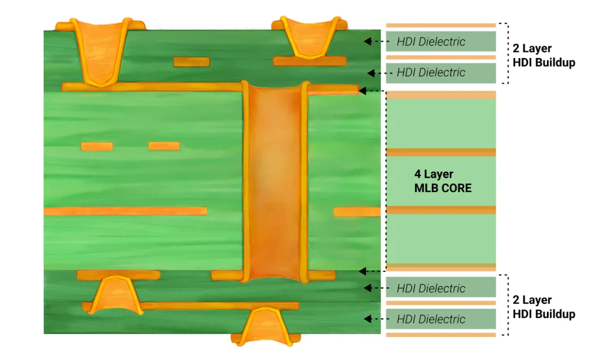
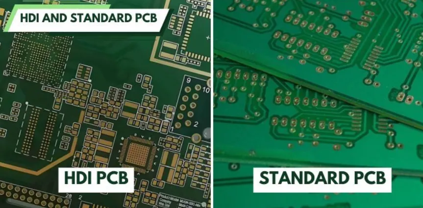
High-density interconnect (HDI) PCBs are engineered to pack more components and connections into a smaller area. A key feature of HDI designs is the use of microvias—tiny holes that connect layers of the board. When these microvias are placed directly on top of each other across multiple layers, they form what’s known as stacked vias. This technique is a game-changer for HDI PCB stacked via design because it saves space and allows for more complex routing in a smaller footprint.
Why does this matter? In modern electronics, from smartphones to medical devices, space is at a premium. Stacked vias help designers achieve higher density without increasing the board size. They also improve signal integrity by shortening connection paths, which can reduce signal loss and interference. For instance, in high-speed applications, shorter paths can lower impedance mismatches, often keeping values below 50 ohms for critical signals.
The Basics of High-Density Interconnect PCB Technology
Before diving deeper into stacked vias, let’s cover the foundation of high-density interconnect PCB technology. HDI boards differ from traditional PCBs by using finer traces, smaller vias, and denser layouts. They often incorporate blind and buried vias, which don’t pass through the entire board, saving even more space compared to through-hole vias.
HDI technology is defined by its ability to support a higher number of connections per unit area. This is often measured by line widths and spacing, which can go as low as 3 mils (0.003 inches) in advanced designs. The result? You can fit more functionality into devices without sacrificing performance. HDI is especially crucial for applications like 5G technology, where signal speeds can exceed 10 Gbps, demanding precise routing and minimal interference.
How Stacked Microvia PCB Manufacturing Works
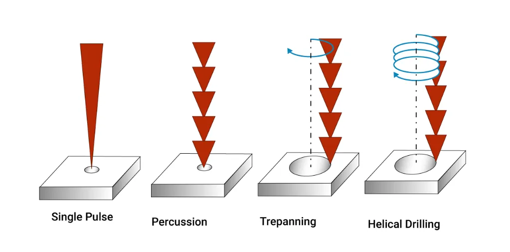
The process of stacked microvia PCB manufacturing is a precise and advanced technique. Microvias are typically laser-drilled, allowing for diameters as small as 3 to 6 mils, much smaller than traditional mechanical drilling can achieve. In a stacked via setup, these microvias are aligned and built layer by layer during the PCB fabrication process.
Here’s a simplified breakdown of the manufacturing steps:
- Layer Build-Up: The board starts with a core layer, and additional layers are added sequentially. Each layer can include microvias to connect to the layer below.
- Laser Drilling: High-precision lasers create microvias at exact locations, ensuring alignment for stacking.
- Copper Filling: Microvias are filled with copper to create a solid electrical connection. This also strengthens the structure for stacking.
- Stacking: Multiple microvias are aligned vertically across layers, forming a stacked via that connects several layers without taking up extra horizontal space.
This method is critical for complex designs where space is limited. However, it requires careful planning to ensure reliability, as misaligned vias or poor copper filling can lead to connection failures. Advanced manufacturing often adheres to standards like IPC-2226, ensuring quality and consistency in HDI production.
Benefits of Stacked Vias in HDI PCB Stacked Via Design
Stacked vias bring several advantages to HDI PCB stacked via design, making them a preferred choice for compact, high-performance electronics. Let’s explore some key benefits:
1. Space Efficiency
By stacking vias vertically, you free up horizontal space on the board. This allows for tighter component placement and smaller overall board dimensions. For example, in a 6-layer HDI board, stacked vias can reduce the need for additional routing layers, cutting down the board’s thickness by up to 30% in some cases.
2. Improved Signal Integrity
Shorter connection paths mean less signal delay and reduced risk of interference. In high-speed designs, stacked vias can help maintain signal integrity by minimizing stub effects—unwanted reflections that occur with longer via paths. This is vital for applications like DDR4 memory, where signal timing must be precise within nanoseconds.
3. Enhanced Thermal Management
Stacked vias can also aid in heat dissipation by providing direct paths for thermal energy to move through layers. This is especially useful in densely packed boards where heat buildup is a concern.
PCB Layer Count Reduction with Stacked Vias
One of the standout advantages of using stacked vias is PCB layer count reduction. Traditional PCB designs often require additional layers to accommodate complex routing. Each added layer increases cost, manufacturing time, and board thickness. With HDI technology and stacked vias, you can achieve the same level of connectivity with fewer layers.
For instance, a design that might require 10 layers in a standard PCB could potentially be reduced to 6 or 8 layers using HDI with stacked vias. This is done by leveraging blind and buried vias alongside stacked structures to maximize vertical connections. Reducing layer count not only lowers production costs—sometimes by 20% or more per board—but also results in a thinner, lighter product, which is critical for portable devices.
Advanced PCB Routing Techniques for HDI Designs
Routing in HDI PCBs is a complex task that requires precision and innovative strategies. Advanced PCB routing techniques are essential to fully utilize the benefits of stacked vias and microvia technology. Here are some approaches commonly used in HDI designs:
1. Via-in-Pad Design
Placing vias directly under component pads saves space and shortens signal paths. This technique, often paired with stacked vias, is ideal for fine-pitch components like ball grid arrays (BGAs) with pin spacing as tight as 0.4 mm.
2. Blind and Buried Vias
These vias don’t extend through the entire board, allowing for more flexible routing on outer layers. When combined with stacked vias, they enable denser layouts without increasing layer count.
3. Fine-Line Routing
HDI boards often use trace widths and spacing below 4 mils. This requires careful impedance control to prevent signal degradation, especially in high-frequency applications operating at 5 GHz or higher.
4. Backdrilling Elimination
In traditional PCBs, backdrilling removes unused via stubs to improve signal quality. With stacked microvias, stubs are naturally minimized, reducing the need for this extra step and saving on manufacturing costs.
These techniques, when applied thoughtfully, can significantly enhance the performance of your HDI designs. They require advanced design software and close collaboration with fabrication teams to ensure manufacturability and reliability.
Challenges in Stacked Via PCB Design and Manufacturing
While stacked vias offer incredible benefits, they also come with challenges that designers and manufacturers must address:
- Alignment Precision: Stacking microvias requires exact alignment across layers. Even a slight offset can lead to connection failures or reduced reliability.
- Cost Considerations: The advanced processes involved, like laser drilling and sequential lamination, can increase production costs compared to standard PCBs, especially for low-volume runs.
- Reliability Concerns: Stacked vias undergo thermal and mechanical stress during operation. Poor copper filling or material choices can lead to cracks or delamination over time.
To mitigate these issues, designers should work closely with fabrication partners to select appropriate materials and processes. For example, using high-Tg (glass transition temperature) materials above 170°C can improve thermal stability in demanding applications.
Applications of Stacked Via HDI PCBs
The use of stacked vias in high-density interconnect PCB designs is transforming industries that rely on compact, high-performance electronics. Some key applications include:
- Consumer Electronics: Smartphones, tablets, and wearables use HDI PCBs to fit powerful components into tiny spaces.
- Telecommunications: 5G infrastructure and high-speed networking equipment rely on HDI for fast, reliable signal transmission.
- Medical Devices: Miniaturized devices like pacemakers and imaging equipment benefit from the space-saving and precision of stacked vias.
- Automotive Systems: Advanced driver-assistance systems (ADAS) and infotainment units use HDI PCBs to handle complex electronics in harsh environments.
Tips for Designing HDI PCBs with Stacked Vias
If you’re new to designing with stacked vias, here are some practical tips to ensure success:
- Plan Your Stack-Up Early: Define the number of layers and via structures at the start to avoid costly redesigns. Aim for a balanced stack-up to minimize warping.
- Optimize Via Placement: Place stacked vias strategically to avoid overcrowding and ensure easy routing. Keep high-speed signals away from densely packed areas.
- Collaborate with Manufacturers: Engage with your fabrication team to confirm capabilities for microvia drilling and copper filling. Verify their ability to handle tight tolerances, such as via aspect ratios below 0.75:1.
- Test for Reliability: Use thermal cycling and stress testing to validate the durability of stacked vias in your design, especially for high-reliability applications.
Conclusion: Unlocking the Future of PCB Design with Stacked Vias
Stacked vias are a cornerstone of modern HDI PCB stacked via design, enabling engineers to push the boundaries of density and performance. By leveraging stacked microvia PCB manufacturing, achieving PCB layer count reduction, and applying advanced PCB routing techniques, you can create compact, high-performing boards for cutting-edge applications. While challenges like precision and cost exist, the benefits of space efficiency, signal integrity, and thermal management make stacked vias a powerful tool in high-density interconnect PCB technology.
At ALLPCB, we’re committed to helping you navigate the complexities of HDI design. Whether you’re working on consumer gadgets or critical industrial systems, our expertise and advanced manufacturing capabilities can bring your vision to life. Start exploring the possibilities of stacked via technology today and unlock new levels of density in your designs!


