ALLPCB


Soldering defects on printed circuit boards (PCBs) can lead to malfunctioning electronics, costly repairs, and project delays. If you're looking for reliable ways to identify and fix these issues, using International Electrotechnical Commission (IEC) testing methods can provide a structured and standardized approach. In this comprehensive guide, we’ll explore how to troubleshoot common soldering defects using IEC standards, offering practical solutions for engineers and technicians in the electronics field. Whether you're dealing with cold solder joints or bridging, this blog will walk you through identifying soldering issues with IEC guidelines, troubleshooting PCB solder joints, and preventing soldering problems in electronics.
Why Soldering Defects Matter in Electronics
Soldering is the backbone of PCB assembly, ensuring components are securely connected to create functional circuits. However, even small defects in soldering can cause major issues like intermittent connections, signal loss, or complete circuit failure. According to industry studies, soldering defects account for nearly 60% of PCB assembly failures. This makes identifying and resolving these issues critical for maintaining product reliability and performance.
The IEC, a global organization that sets standards for electrical and electronic technologies, provides detailed guidelines for testing and quality assurance. Using IEC soldering defect analysis methods ensures that your troubleshooting process is consistent, repeatable, and aligned with international best practices. Let’s dive into the common soldering defects and how IEC standards can help address them.
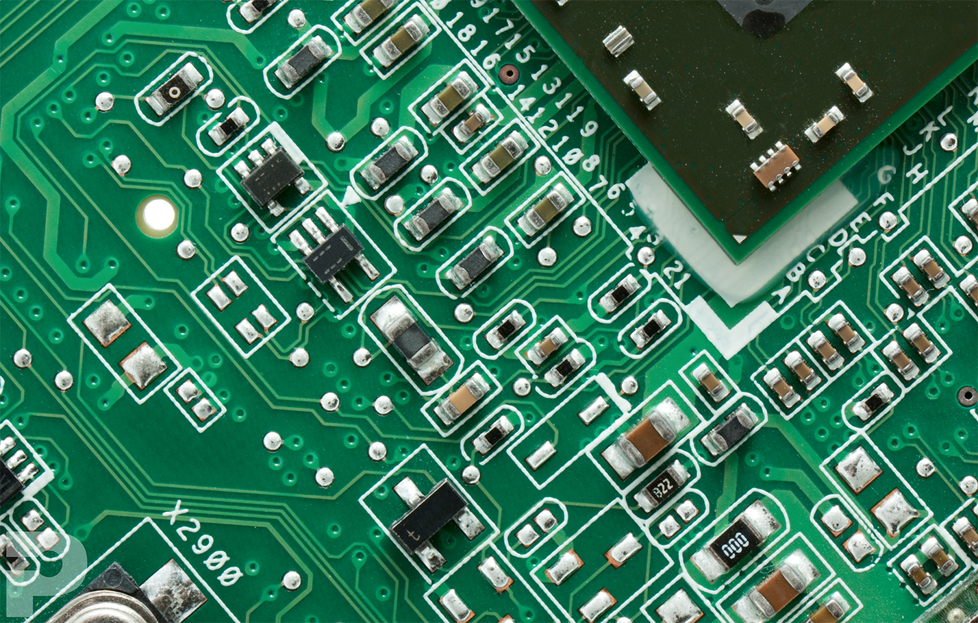
Common Soldering Defects in PCB Assembly
Before applying IEC testing methods, it’s important to understand the most frequent soldering issues encountered in electronics manufacturing. Below are some of the key defects that can compromise PCB performance:
- Cold Solder Joints: These occur when the solder doesn’t fully melt, resulting in a weak, grainy connection. They often lead to intermittent electrical conductivity, with resistance values sometimes exceeding 10 ohms in affected joints.
- Solder Bridging: This happens when excess solder creates an unintended connection between two pads or pins, causing short circuits. This defect can disrupt signal integrity, especially in high-frequency circuits operating above 100 MHz.
- Insufficient Solder: Too little solder can result in poor mechanical and electrical connections, increasing the risk of joint failure under stress or vibration.
- Tombstoning: This defect occurs when a component stands upright on one end due to uneven heating during reflow soldering, leaving one side disconnected.
- Cracked Joints: Often caused by thermal stress or mechanical shock, cracked solder joints can lead to open circuits, with failure rates increasing by up to 30% in harsh environments.
Each of these defects poses unique challenges, but IEC standards provide a framework for identifying and addressing them systematically.
Understanding IEC Standards for Solder Defects
The IEC offers a range of standards that apply to soldering and PCB assembly, ensuring quality and reliability in electronics. One key standard relevant to soldering defect analysis is IEC 61191, which covers printed board assemblies. This standard outlines requirements for materials, processes, and testing methods to ensure soldered connections meet quality benchmarks.
Another important reference is IEC 60068, which includes environmental testing procedures that can reveal soldering defects under stress conditions like temperature cycling or vibration. These standards help in identifying soldering issues with IEC-approved methods by setting clear criteria for acceptable solder joint appearance, mechanical strength, and electrical performance. For instance, IEC guidelines specify that a proper solder joint should exhibit a smooth, shiny surface with a fillet angle between 30 and 45 degrees for optimal bonding.
By adhering to the IEC standard for solder defects, manufacturers can establish consistent inspection and troubleshooting processes, reducing the likelihood of defective products reaching the market.

Step-by-Step Guide to Troubleshooting PCB Solder Joints with IEC Methods
Troubleshooting PCB solder joints using IEC testing methods involves a systematic approach to detect, analyze, and resolve defects. Below is a detailed step-by-step process to guide you through IEC soldering defect analysis:
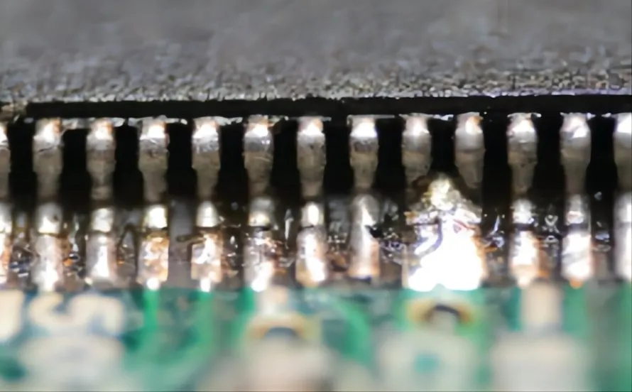
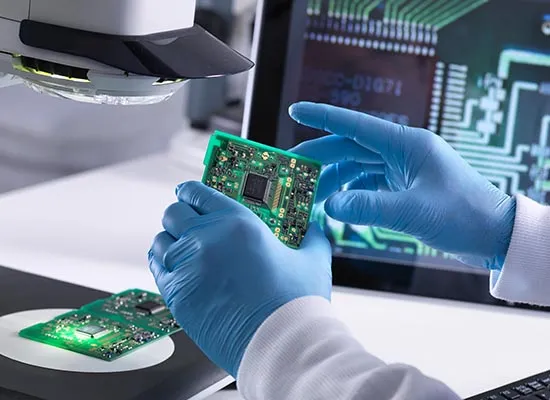
Step 1: Visual Inspection
Start with a thorough visual inspection as outlined in IEC 61191. Use a magnifying glass or microscope to examine solder joints for visible defects like cracks, bridges, or dull appearances indicative of cold joints. IEC standards recommend a minimum magnification of 10x for detailed inspection. Look for uniformity in solder fillets and ensure there are no visible gaps or irregularities.
Step 2: Electrical Testing
Electrical testing is critical for identifying soldering issues with IEC methods. Use a multimeter to check for continuity and resistance across solder joints. According to IEC guidelines, resistance in a healthy joint should typically be below 1 ohm. High resistance readings may indicate a cold joint or insufficient solder, while a short circuit reading could point to bridging.
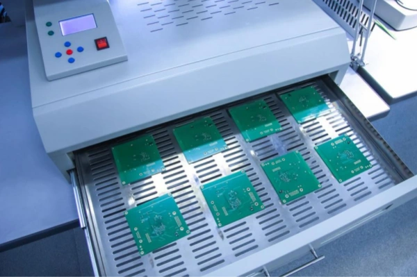
Step 3: Thermal Stress Testing
IEC 60068-2-14 provides protocols for thermal cycling tests to expose weaknesses in solder joints. Subject the PCB to temperature extremes, such as cycling between -40°C and 85°C for 100 cycles, to simulate real-world conditions. Monitor for changes in electrical performance or visible cracks that may develop due to thermal expansion and contraction.
Step 4: Mechanical Stress Testing
Mechanical stress tests, also covered under IEC 60068, involve subjecting the PCB to vibration or shock to evaluate solder joint durability. For example, apply a vibration frequency of 10-55 Hz for 2 hours to detect loose or cracked joints. IEC standards specify acceptable limits for displacement and failure rates during these tests.
Step 5: Advanced Imaging Techniques
For deeper analysis, use X-ray imaging to inspect hidden solder joints, especially in surface-mount technology (SMT) assemblies. IEC standards support the use of non-destructive testing methods to identify internal voids or insufficient solder without damaging the board. Ensure the X-ray equipment meets IEC safety and calibration requirements for accurate results.
Step 6: Rework and Repair
Once defects are identified, follow IEC guidelines for rework. Use a soldering iron with controlled temperature settings (typically 300-350°C for lead-free solder) to reflow or remove defective solder. Ensure proper cleaning of the area with isopropyl alcohol and apply fresh solder to create a reliable joint. IEC standards emphasize minimizing thermal stress during rework to avoid further damage.
Preventing Soldering Problems in Electronics
While troubleshooting is essential, preventing soldering problems in electronics is equally important for long-term reliability. By following IEC standards and best practices, you can minimize defects during the assembly process. Here are some actionable tips:
- Optimize Soldering Temperature: Maintain soldering iron or reflow oven temperatures within IEC-recommended ranges (260-350°C for most alloys) to avoid cold joints or component damage. Overheating can degrade components, with failure rates increasing by 20% for every 50°C above the recommended limit.
- Use Quality Materials: Select solder alloys and fluxes that comply with IEC material standards to ensure consistent performance. Poor-quality materials can lead to defects like voids or weak joints.
- Control Reflow Profiles: For SMT assembly, design reflow profiles based on IEC guidelines to ensure even heating and cooling. Uneven profiles often cause tombstoning or bridging, with defect rates as high as 15% in poorly controlled processes.
- Train Personnel: Ensure technicians are trained in IEC-compliant soldering techniques. Proper handling and soldering skills can reduce human-induced defects by up to 40%, according to industry reports.
- Implement Regular Inspections: Conduct in-process inspections using IEC testing methods to catch defects early. Automated optical inspection (AOI) systems, aligned with IEC standards, can detect up to 95% of visible soldering issues before final assembly.
Benefits of Using IEC Standards for Soldering Defect Analysis
Adopting IEC standards for troubleshooting and preventing soldering defects offers several advantages for electronics manufacturers:
- Consistency: IEC methods provide a uniform approach to testing and repair, ensuring consistent results across different projects and teams.
- Reliability: Products tested under IEC guidelines are more likely to meet customer expectations, with failure rates reduced by up to 25% in compliant assemblies.
- Global Acceptance: IEC standards are recognized worldwide, making it easier to meet regulatory requirements and gain market trust.
- Cost Savings: Early detection and prevention of defects using IEC methods can save significant costs associated with rework and warranty claims, with potential savings of 10-20% on production expenses.
Conclusion: Mastering Soldering Defect Troubleshooting with IEC Standards
Soldering defects can be a major hurdle in PCB assembly, but with the right approach, they don’t have to be. By leveraging IEC testing methods for soldering defect analysis, you can systematically identify and resolve issues like cold joints, bridging, and insufficient solder. Following IEC standards not only helps in troubleshooting PCB solder joints but also plays a crucial role in preventing soldering problems in electronics, ensuring high-quality and reliable products.
Whether you’re a seasoned engineer or new to electronics manufacturing, integrating IEC guidelines into your workflow can elevate your quality control processes. From visual inspections to advanced thermal and mechanical testing, these methods provide a comprehensive toolkit for addressing soldering challenges. Start implementing these practices today to build robust, defect-free PCBs that stand the test of time.