 ALLPCB


When it comes to PCB gold finger plating, two methods stand out: Electroless Nickel Immersion Gold (ENIG) and Electroplating. If you're wondering which is better for your project, the quick answer is that it depends on your needs. ENIG offers excellent corrosion resistance and solderability, making it ideal for many applications, while Electroplating (often as Hard Gold or Soft Gold) provides durability for high-wear areas like connectors. However, costs, performance, and specific drawbacks differ significantly. In this detailed guide, we'll break down the benefits, drawbacks, cost analysis, and performance of both methods to help you make an informed decision for your PCB designs.
What Are PCB Gold Fingers and Why Do They Matter?
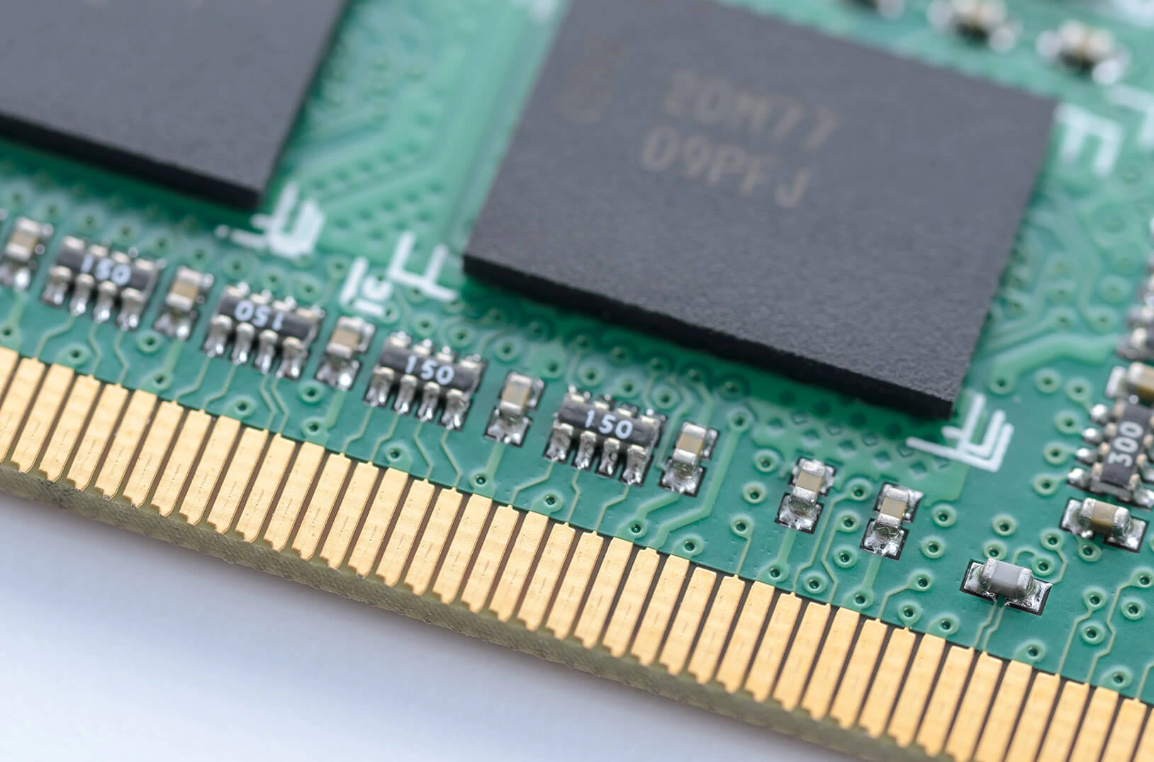
Gold fingers are the gold-plated connectors on the edge of a printed circuit board (PCB). They are essential for ensuring reliable electrical connections, especially in devices where boards are frequently inserted and removed, such as computer memory modules or expansion cards. Gold is used because it resists corrosion, provides excellent conductivity, and maintains signal integrity over time.
The plating method used for gold fingers directly impacts the PCB's performance, durability, and cost. Choosing between ENIG and Electroplating is a critical decision that can affect the lifespan and reliability of your product. Let’s dive into the specifics of each method to understand their strengths and weaknesses.
Understanding ENIG (Electroless Nickel Immersion Gold)
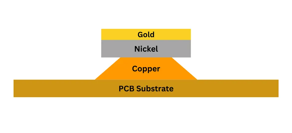
ENIG is a two-layer plating process that involves applying a layer of nickel followed by a thin layer of gold through a chemical reaction, without the use of an electric current. This method is widely used in PCB manufacturing for its uniform coating and compatibility with various applications.
Benefits of ENIG for Gold Fingers
- Corrosion Resistance: The nickel underlayer in ENIG acts as a barrier, protecting the copper beneath from oxidation and ensuring long-term reliability.
- Excellent Solderability: ENIG provides a flat, smooth surface that is ideal for soldering components, which is crucial for surface mount technology (SMT) applications.
- Uniform Thickness: Since it’s a chemical process, ENIG ensures consistent gold thickness, typically between 0.05 to 0.1 micrometers, across the entire surface, reducing the risk of uneven wear.
- Cost-Effective for Large Areas: ENIG can be more economical when plating larger surfaces or multiple areas of a PCB, as it doesn’t require complex setups like Electroplating.
Drawbacks of ENIG
- Limited Durability for High-Wear: The thin gold layer in ENIG (often less than 0.1 micrometers) can wear off in applications with frequent insertions, such as gold fingers on memory cards, leading to potential signal loss.
- Black Pad Issue: A known concern with ENIG is the "black pad" defect, where nickel corrosion during the gold immersion process can lead to poor solder joints and reduced reliability.
- Not Ideal for Thick Gold Layers: If a thicker gold layer is needed for durability, ENIG may not be the best choice, as it’s challenging to achieve thicknesses beyond 0.1 micrometers.
Understanding Electroplating (Hard Gold and Soft Gold)
Electroplating, also known as electrolytic plating, uses an electric current to deposit a layer of gold onto the PCB surface, often over a nickel base layer. This method is commonly used for gold fingers and is categorized into Hard Gold (alloyed with other metals for durability) and Soft Gold (pure gold for specific applications).
Benefits of Electroplating for Gold Fingers
- High Durability: Hard Gold plating, with thicknesses ranging from 0.8 to 1.5 micrometers or more, is designed for high-wear applications. It can withstand thousands of insertion cycles (up to 20,000 in some cases) without significant wear, making it perfect for connectors and edge contacts.
- Customizable Thickness: Electroplating allows precise control over gold thickness, which can be tailored based on the application’s needs, from thin layers for cost savings to thick layers for durability.
- Superior Contact Performance: The thicker gold layer ensures low contact resistance, maintaining signal integrity even under harsh conditions or high-frequency signals (up to 10 GHz in some designs).
Drawbacks of Electroplating
- Higher Cost: Electroplating, especially Hard Gold, is more expensive due to the amount of gold used and the complexity of the process. Costs can be 2-3 times higher than ENIG for the same area.
- Poor Solderability: Hard Gold is not ideal for soldering because of its alloyed composition, which can lead to brittle joints. Soft Gold offers better solderability but is less durable for high-wear applications.
- Non-Uniform Coating: Unlike ENIG, Electroplating may result in uneven gold distribution, especially on complex geometries, potentially affecting performance in critical areas.
Cost Analysis: ENIG vs. Electroplating
Cost is a major factor when deciding between ENIG and Electroplating for PCB gold fingers. Let’s break down the cost implications for each method.
- ENIG Costs: ENIG is generally more affordable for larger surface areas or full-board plating. The process costs are lower because it doesn’t require electrical setups or extensive gold material. For a standard PCB, ENIG plating might cost around $0.50 to $1.00 per square inch, depending on volume and board complexity. However, if rework is needed due to issues like black pad, costs can increase.
- Electroplating Costs: Electroplating, particularly Hard Gold, is pricier due to the higher gold content and labor-intensive setup. Costs can range from $1.50 to $3.00 per square inch or more, especially for thicker layers. For small areas like gold fingers, selective plating can reduce expenses, but the overall price remains higher than ENIG.
In summary, if budget is a primary concern and your application doesn’t require frequent insertions, ENIG might be the better choice. For high-durability needs, the higher cost of Electroplating could be a worthwhile investment.
Performance Comparison: ENIG vs. Electroplating
Performance is where these two methods truly differ, as each excels in specific scenarios. Let’s compare key performance metrics for gold fingers.
Durability and Wear Resistance
Electroplating with Hard Gold is the clear winner for durability. It’s designed for applications with high mechanical stress, enduring up to 20,000 insertion cycles without significant degradation. ENIG, with its thinner gold layer, typically lasts for only a few hundred cycles before wear exposes the nickel layer, increasing contact resistance.
Signal Integrity and Conductivity
Both methods provide excellent conductivity due to gold’s low resistivity (2.44 × 10^-8 Ω·m). However, Electroplating can maintain lower contact resistance over time, especially in thicker applications, ensuring minimal signal loss for high-frequency designs (up to 10 GHz). ENIG performs well initially but may degrade faster in high-wear scenarios, potentially affecting signals above 5 GHz.
Solderability
ENIG outperforms Electroplating in solderability. Its smooth, thin gold layer dissolves easily during soldering, creating strong joints with lead-free solders. Hard Gold, due to its alloyed nature, often results in weaker solder joints, while Soft Gold is better but less common for gold fingers due to durability concerns.
Corrosion Resistance
Both methods offer excellent corrosion resistance thanks to gold’s inert properties. ENIG’s nickel underlayer provides an additional barrier, making it highly resistant to environmental factors like humidity (up to 85% RH in testing). Electroplating also resists corrosion well, though thicker layers are needed to prevent pinholes that could expose underlying metals.
Application Scenarios: When to Choose ENIG or Electroplating
Choosing the right plating method depends on your specific application. Here are some guidelines based on common use cases.
- Choose ENIG If: Your PCB requires excellent solderability, such as in SMT-heavy designs, or if you’re plating larger areas where cost savings are critical. ENIG is also suitable for low-wear gold fingers, like in single-use or low-insertion devices.
- Choose Electroplating If: Your application involves frequent insertions, such as memory modules or industrial connectors, where durability is non-negotiable. Hard Gold is ideal for high-reliability products, even at a higher cost.
For example, a consumer electronics PCB with minimal edge connector usage might benefit from ENIG to keep costs down. On the other hand, a server-grade memory module requiring thousands of insertions would be better served by Hard Gold Electroplating to ensure longevity.
Key Considerations for PCB Design and Manufacturing
Beyond cost and performance, there are a few design and manufacturing factors to keep in mind when selecting a plating method for gold fingers.
- Thickness Requirements: Determine the minimum gold thickness needed for your application. Standards like IPC-6012 suggest 0.8 micrometers for Hard Gold in high-wear areas, while ENIG’s typical 0.05-0.1 micrometers suits less demanding uses.
- Selective Plating: For cost efficiency, consider selective plating for gold fingers only, especially with Electroplating, to avoid unnecessary gold usage on non-critical areas.
- Environmental Conditions: If your PCB will operate in harsh environments (high humidity or temperature swings), prioritize corrosion resistance and test both methods under simulated conditions.
Conclusion: Making the Right Choice for Your PCB Gold Fingers
Deciding between ENIG and Electroplating for PCB gold fingers boils down to balancing cost, performance, and application needs. ENIG shines in scenarios requiring solderability and affordability, with excellent corrosion resistance for general use. Electroplating, particularly Hard Gold, is the go-to choice for high-durability needs, ensuring reliable performance in demanding, high-wear applications despite its higher cost.
By understanding the benefits, drawbacks, cost implications, and performance differences, you can select the plating method that best aligns with your project goals. Whether you prioritize long-term reliability or budget constraints, both ENIG and Electroplating offer unique advantages to enhance your PCB designs. Partnering with a trusted manufacturing service can further ensure that your chosen method is applied with precision and quality, delivering a product that meets your expectations.


