 ALLPCB


Introduction
Audio amplifiers form the heart of many hobbyist projects, from simple guitar pedals to full home stereo systems. For electronic hobbyists, achieving clear sound with minimal distortion requires careful attention to PCB design. Through-hole design audio approaches offer unique advantages in handling power and heat, which are critical for amplifier circuits. Unlike surface-mount options, through-hole components provide robust mechanical connections and easier prototyping on a bench setup. This article explores through-hole amplifier circuit strategies to optimize performance. Hobbyists can apply these principles to build reliable boards that deliver high-fidelity audio.
Why Through-Hole Design Matters for Audio Amplifiers
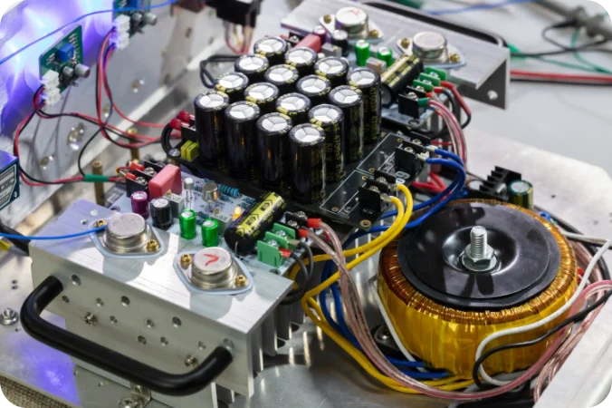
Through-hole technology uses components with leads that pass through drilled holes in the PCB and are soldered on the opposite side. In audio applications, this method excels where high current flows and thermal dissipation are essential. Hobbyists often choose through-hole for amplifiers because it supports larger components like power transistors and electrolytic capacitors, which handle the demands of audio signals better. Surface-mount might suit compact devices, but through-hole provides superior vibration resistance, ideal for speaker enclosures or portable amps.
The relevance grows with hobby projects involving discrete transistors or op-amps in Class A or AB configurations. Poor design can lead to hum, crosstalk, or overheating, ruining the listening experience. Through-hole design audio ensures signal integrity by allowing wider traces and better heat spreading. For electronic hobbyists prototyping at home, the solderability simplifies testing and modifications without specialized reflow ovens.
Standards like IPC-2221B guide trace width calculations to prevent voltage drops in power paths. This structured approach helps hobbyists avoid common pitfalls. Ultimately, through-hole amplifier circuit design balances cost, performance, and ease of assembly for satisfying results.
Key Technical Principles in Through-Hole Amplifier Circuit Design
Effective through-hole design audio starts with understanding signal flow and impedance matching. Audio signals range from millivolts to tens of volts, so layouts must minimize noise pickup through short, direct paths for low-level inputs. Place sensitive preamp stages away from power supply lines to reduce electromagnetic interference. Ground planes, even partial ones under through-hole boards, shield against stray fields and provide low-impedance returns.
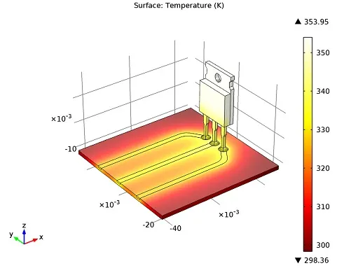
Power distribution demands thick copper traces for output stages. For a typical 50W amplifier, traces carrying several amps need widths calculated based on current density, often 1-2 oz copper or more. Through-hole vias connect layers efficiently, but oversize them to handle heat without cracking solder joints. Component orientation matters: align heat-generating parts like BJTs toward board edges for sink mounting.
Thermal management follows principles in IPC-6012E, ensuring boards withstand operating temperatures without delamination. Hobbyists should space high-power resistors and inductors to allow airflow. Decoupling capacitors near IC pins filter ripple, using through-hole ceramics or films for audio paths. These mechanisms ensure stable bias points and low THD.
Grounding schemes define performance in through-hole amplifier circuits. Star grounding converges all returns at one point to avoid loops inducing hum at 60Hz. For multi-stage amps, separate analog and power grounds, tying them at the rectifier output. This prevents feedback modulation. Bypass capacitors bridge sections strategically.
Best Practices for Audio Amplifier PCB Design Through-Hole
Begin with schematic capture, verifying gain stages and feedback loops before layout. Use 1.6mm FR-4 thickness for standard hobbyist boards, providing rigidity under component stress. Pad sizes follow J-STD-001 guidelines: 0.8-1.2mm annular rings for 0.8mm holes suit most leads. Annular rings prevent lift-off during soldering.
Trace routing prioritizes signal integrity in through-hole design audio. Keep input traces on the top layer, away from output swings. Route power and ground as wide pours, stitching with vias every 10-20mm. For op-amp based amps, twin-lead routing for differential inputs reduces common-mode noise. Avoid right angles in high-frequency paths, though audio below 20kHz tolerates them.
Component placement groups functions logically: inputs left, outputs right, power center. Mount TO-220 transistors off-board for heatsinks, using insulated bushings. Electrolytic caps orient with negative leads toward ground pours. Silk screen labels clearly for troubleshooting. These practices yield low-noise through-hole amplifier circuits.
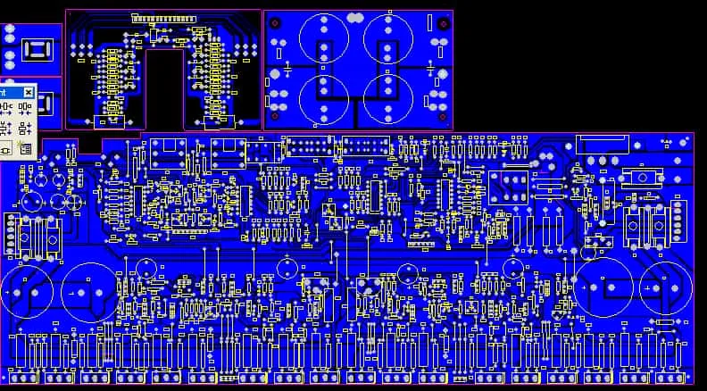
Layer stackup simplifies to single or double-sided for hobbyists. Double-sided enables ground planes underneath, improving shielding. Via fencing around sensitive areas blocks fields. Solder mask over traces prevents shorts, leaving pads exposed. Bake boards pre-assembly if humidity exceeds 60% to avoid popcorn effects.
Testing iterates design: measure DC offsets, frequency response, and distortion. Use oscilloscopes for stability checks. Adjust feedback resistors if oscillation appears. These steps refine audio amplifier PCB design through-hole for optimal sound.
Common Challenges and Troubleshooting in Through-Hole Audio Builds
Hobbyists face hum from ground loops in through-hole amplifier circuits. Solution: verify star points with multimeter continuity. Lifted pads occur from thermal mismatch; use flux and preheat gently. Overheating transistors signal inadequate trace widths, recalculate per current needs.
Crosstalk plagues multi-channel amps. Space channels 5-10mm apart, shield with ground traces. Electrolytic cap failures from reverse polarity demand diode protection in supplies. Oscillation from parasitic inductance requires snubbers across inductors. Systematic checks resolve most issues.
Poor soldering causes intermittent contacts. Clean leads, use 60/40 solder at 350C. Inspect fillets per IPC-A-600 criteria for acceptability. These fixes ensure reliable performance.
Conclusion
Through-hole design audio empowers hobbyists to craft high-performance amplifiers with accessible tools. Key principles like strategic grounding, thermal planning, and trace optimization minimize noise and distortion. Best practices from component placement to testing deliver boards ready for enclosures. Standards such as IPC-2221B and J-STD-001 provide the foundation for consistent results. Experiment iteratively to refine through-hole amplifier circuit designs. Enjoy the satisfaction of pure, powerful sound from your custom builds.
FAQs
Q1: What is through-hole design audio, and why choose it for amplifiers?
A1: Through-hole design audio involves components with leads soldered through PCB holes, ideal for hobbyist audio amplifiers needing high power handling. It offers better heat dissipation and mechanical strength than surface-mount for output transistors. Easier hand-soldering suits prototyping. This approach ensures low distortion in through-hole amplifier circuits.
Q2: How does audio amplifier PCB design through-hole improve signal quality?
A2: Audio amplifier PCB design through-hole uses wide traces and ground planes to reduce noise pickup. Short signal paths and decoupling caps filter ripple effectively. Star grounding eliminates hum common in amps. Hobbyists achieve cleaner sound with proper layout.
Q3: What are common mistakes in through-hole amplifier circuit layouts?
A3: Common mistakes include long ground loops causing 60Hz hum and undersized power traces leading to drops. Poor component spacing invites crosstalk. Ignoring via stitching weakens shielding. Follow spacing and width rules for reliable through-hole design audio.
Q4: Can hobbyists use double-sided boards for through-hole design audio?
A4: Yes, double-sided boards enhance through-hole design audio with ground planes for shielding. Stitch pours with vias for low impedance. This setup suits multi-stage amps, improving noise rejection. Keep it simple for home etching or ordering.
References
IPC-2221B — Generic Standard on Printed Board Design. IPC, 2009
IPC-6012E — Qualification and Performance Specification for Rigid Printed Boards. IPC, 2017
J-STD-001G — Requirements for Soldered Electrical and Electronic Assemblies. IPC, 2011


