ALLPCB


If you're dealing with PCB pad lifting, you're likely facing a frustrating issue that can disrupt the functionality of your printed circuit board. But what is pad lifting, and how can you fix or prevent it? In short, PCB pad lifting occurs when the copper pad on a circuit board detaches from the surface, often due to thermal or mechanical stress, leading to poor connections or component failure. This comprehensive guide will dive deep into the causes, solutions, and prevention strategies for pad lifting, ensuring your boards remain reliable and efficient.
Whether you're searching for a PCB pad lifting guide, a pad lifting tutorial, or just a clear pad lifting overview, this article has you covered. We'll break down everything you need to know about pad lifting explained in simple terms, with actionable tips to tackle this common problem. Let's get started on understanding and solving pad lifting issues for good.
What Is Pad Lifting on a PCB?
Pad lifting is a common issue in printed circuit boards (PCBs) where the copper pad—a small, flat area of metal used to connect components to the board—detaches or lifts from the board's surface. These pads are critical for creating electrical connections between components like resistors, capacitors, or integrated circuits and the copper traces on the PCB. When a pad lifts, the connection becomes unreliable or completely fails, which can lead to malfunctioning electronics.
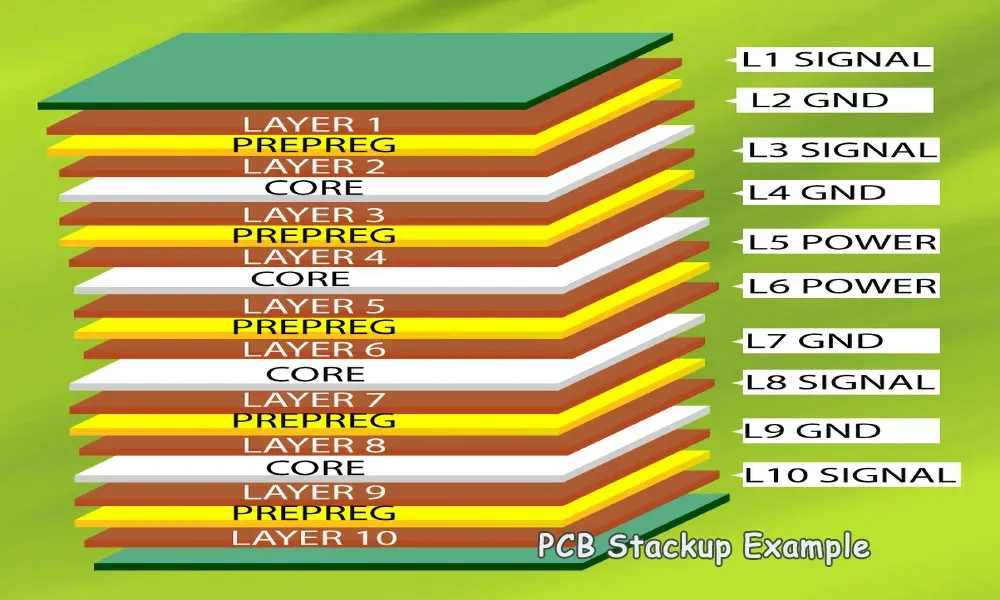
This problem is often more prevalent in single-layer boards, where the pad adhesion to the substrate may not be as robust as in multi-layer designs. Understanding what is pad lifting is the first step to addressing it, and recognizing its impact on your project can help you prioritize solutions.
Common Causes of PCB Pad Lifting
To effectively combat pad lifting, it's essential to understand why it happens. Several factors contribute to this issue, ranging from design flaws to handling errors. Below, we explore the most common causes of PCB pad lifting to help you identify potential risks in your process.
1. Thermal Stress During Soldering
One of the primary reasons for pad lifting is thermal stress. During soldering, especially in reflow or wave soldering processes, the PCB is exposed to high temperatures (often exceeding 250°C). If the pad or the surrounding laminate material cannot withstand this heat, the adhesive bond between the pad and the board weakens, causing the pad to lift. This is particularly common when soldering is done repeatedly or if the soldering iron tip is too hot, exceeding 300°C for prolonged periods.
2. Mechanical Stress from Handling
Physical stress is another major cause. Mishandling during assembly, rework, or even transportation can exert excessive force on the pads. For instance, using too much pressure while desoldering a component or accidentally bending the board can cause the pad to detach. Thin or poorly designed pads are especially vulnerable to such mechanical stress.
3. Poor Pad Design or Material Quality
The design and quality of the PCB itself play a significant role. If the pad size is too small (e.g., less than 0.5 mm in diameter for certain components), or if the copper thickness is inadequate (typically below 1 oz/ft2), the pad may not adhere properly to the substrate. Additionally, low-quality laminate materials or insufficient adhesive layers can lead to weak bonding, increasing the risk of lifting.
4. Moisture Absorption
Moisture trapped in the PCB material can expand when exposed to high temperatures during soldering, creating internal pressure that lifts the pad. This is often seen in boards stored in humid environments or those not baked before assembly to remove moisture. For example, a board with a moisture content above 0.2% by weight is at higher risk during reflow soldering at 260°C.
Impact of Pad Lifting on PCB Performance
Pad lifting doesn't just affect a single component; it can compromise the entire functionality of your PCB. When a pad lifts, the electrical connection between the component and the board is disrupted, leading to intermittent signals or complete failure. For high-frequency applications, where signal integrity is critical, a lifted pad can introduce impedance mismatches, potentially increasing signal loss by up to 20% or more depending on the circuit design.
In severe cases, lifted pads can cause short circuits if they come into contact with nearby traces or components. This is a significant concern in compact, densely populated boards where spacing between traces might be as tight as 0.1 mm. The reliability of the final product is at stake, making it crucial to address pad lifting promptly.
How to Fix Lifted Pads on a PCB: Step-by-Step Solutions
If you're dealing with a lifted pad, don't worry—there are practical ways to repair it. This pad lifting tutorial section will walk you through a detailed process to restore functionality to your board. These solutions are tailored for engineers and hobbyists looking for actionable steps.
Step 1: Assess the Damage
Start by inspecting the lifted pad under a magnifying glass or microscope. Determine if the pad is completely detached or partially lifted. Check if the underlying trace is still intact. If the trace is damaged, note its location and length (e.g., a 5 mm section) for repair planning.
Step 2: Clean the Area
Use isopropyl alcohol (at least 90% concentration) and a small brush to clean the area around the lifted pad. Remove any debris, solder residue, or oxidation. This ensures a clean surface for repair and prevents contaminants from interfering with adhesion.
Step 3: Reattach the Pad
If the pad is partially lifted, apply a small amount of high-strength epoxy (rated for electronics use with a tensile strength of at least 5000 psi) to secure it back to the board. Use a toothpick or fine applicator to place the epoxy precisely under the pad. Press the pad down gently with tweezers and allow the epoxy to cure as per the manufacturer's instructions, typically 24 hours at room temperature.
Step 4: Repair or Replace the Trace
If the trace connected to the pad is damaged or missing, use a conductive pen or copper foil to recreate the connection. For example, if a 2 mm section of trace is missing, cut a matching piece of copper foil (0.1 mm thick) and bond it with conductive adhesive. Ensure the new trace aligns with the original path to maintain signal integrity.
Step 5: Test the Connection
After the repair, use a multimeter to test continuity between the pad and the connected trace. Verify that resistance is negligible (below 0.1 ohms) to confirm a reliable connection. If a component was attached to the pad, resolder it carefully using a temperature-controlled soldering iron set to around 280°C to avoid further damage.
Preventing PCB Pad Lifting: Best Practices
While repairing a lifted pad is possible, prevention is always better than a cure. Implementing the following best practices can significantly reduce the likelihood of pad lifting in your PCB projects. This pad lifting overview of prevention strategies will help you build more robust boards.
1. Optimize Pad Design
Design pads with adequate size and thickness to handle the mechanical and thermal stresses of assembly. For surface-mount components, ensure pad dimensions follow industry standards, such as a minimum width of 0.6 mm for 0402 resistors. Use teardrop-shaped pads for through-hole components to distribute stress evenly and reduce lifting risks.
2. Use High-Quality Materials
Choose PCB substrates with strong adhesive properties and low moisture absorption rates, such as FR-4 with a glass transition temperature (Tg) of at least 170°C. Opt for copper foils with a thickness of 1.4 oz/ft2 or higher to enhance pad durability.
3. Control Soldering Temperatures
During assembly, maintain soldering temperatures within recommended limits. For lead-free solder, keep reflow profiles below 260°C peak temperature, and limit exposure time to under 10 seconds at peak heat. Use a temperature-controlled soldering iron for manual work, ideally set between 250°C and 300°C, to avoid overheating pads.
4. Store and Handle Boards Properly
Store PCBs in a dry, controlled environment with humidity below 50% to prevent moisture absorption. Use vacuum-sealed bags with desiccant packs if long-term storage is needed. During handling, avoid excessive bending or dropping the board, and use proper tools like anti-static wrist straps to minimize physical stress.
5. Pre-Bake Boards Before Assembly
For boards exposed to humid conditions, pre-bake them at 120°C for 2-4 hours before soldering to remove trapped moisture. This reduces the risk of delamination or pad lifting caused by steam expansion during high-temperature processes.
Advanced Tips for Pad Lifting Prevention in High-Stakes Projects
For engineers working on high-reliability or high-frequency PCB designs, additional measures can further safeguard against pad lifting. Consider implementing via-in-pad designs for better thermal dissipation, reducing heat buildup during soldering. Ensure that your design software accounts for thermal expansion coefficients, matching the pad and substrate materials to minimize stress (e.g., a CTE mismatch of less than 10 ppm/°C).
Additionally, conduct thorough testing under simulated conditions. Use thermal cycling tests between -40°C and 125°C for 1000 cycles to evaluate pad adhesion durability before mass production. Such rigorous testing can identify weak points in your design, allowing for adjustments before costly failures occur.
Conclusion: Mastering PCB Pad Lifting Challenges
PCB pad lifting is a common yet preventable issue that can compromise the performance and reliability of your circuit boards. By understanding what is pad lifting and its root causes—such as thermal stress, mechanical damage, and poor design—you can take proactive steps to mitigate risks. Whether you're following this PCB pad lifting guide to repair a damaged board or using these prevention tips to avoid issues altogether, the key is attention to detail and adherence to best practices.
From optimizing your pad designs to controlling soldering temperatures and handling boards with care, the solutions and strategies outlined in this pad lifting explained article provide a clear path forward. Armed with this knowledge, you can ensure your PCBs perform reliably, even in the most demanding applications. Keep these tips in mind for your next project, and you'll be well on your way to mastering the challenges of pad lifting.