 ALLPCB


If you're new to the world of printed circuit board (PCB) manufacturing or assembly, understanding how to spot issues early can save time, money, and frustration. Visual PCB inspection is a fundamental skill for identifying common defects like solder joint issues, component misplacement, and manufacturing errors. In this guide, we'll walk you through the essentials of manual PCB inspection, highlight frequent PCB defects, and provide practical tips to help you ensure quality in your projects.
Whether you're a hobbyist, a technician, or an engineer just starting out, this comprehensive beginner’s guide will equip you with the knowledge to perform effective visual inspections and recognize problems before they escalate. Let’s dive into the world of PCB defects and inspection techniques to help you achieve reliable and high-quality results.
What Is Visual PCB Inspection and Why Does It Matter?
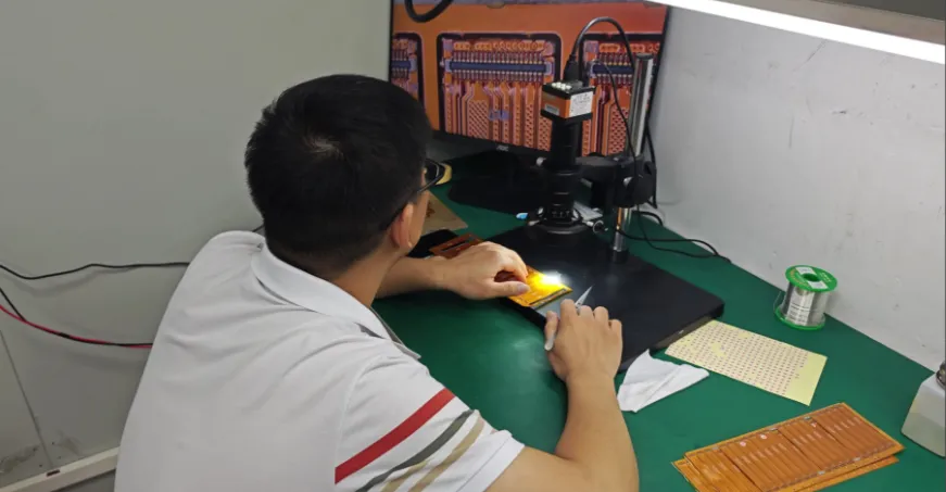
Visual PCB inspection is the process of examining a printed circuit board with the naked eye or basic magnification tools to identify defects or errors in manufacturing and assembly. It’s often the first step in quality control, performed before more advanced testing methods like automated optical inspection (AOI) or electrical testing. This manual inspection is critical because it can catch obvious issues early, preventing costly rework or failures in the final product.
PCBs are the backbone of almost every electronic device, from smartphones to industrial machinery. A single defect, such as a poor solder joint or a misaligned component, can lead to malfunctions or complete system failure. By mastering visual inspection, you ensure that these issues are spotted and addressed promptly, maintaining the reliability and performance of your electronics.
The Basics of Manual PCB Inspection: Tools and Setup
Before you start inspecting a PCB, you need the right tools and environment to make the process effective. Manual PCB inspection doesn’t require expensive equipment, but having the following essentials will improve accuracy:
- Good Lighting: Use a bright, adjustable desk lamp or a ring light to illuminate the PCB surface. Shadows can hide small defects, so ensure even lighting across the board.
- Magnification Tools: A magnifying glass (5x to 10x magnification) or a stereo microscope helps in spotting tiny issues like hairline cracks or solder joint defects.
- Reference Materials: Keep the PCB design files, schematics, or a known good board nearby for comparison.
- Clean Workspace: Work in a dust-free area to avoid contaminating the board during inspection.
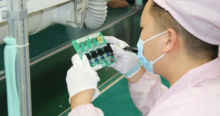
With these tools in place, position the PCB at a comfortable angle and start your inspection systematically. Begin with a general overview of the board, then focus on specific areas like solder joints, traces, and components. Taking your time during manual PCB inspection ensures you don’t miss subtle defects.
Common PCB Defects to Look for During Visual Inspection
During visual PCB inspection, your goal is to identify manufacturing errors and assembly issues that could affect the board’s performance. Below, we’ll cover the most common PCB defects, what they look like, and why they happen. Familiarizing yourself with these issues will make your inspections more effective.
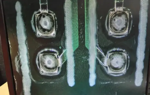
1. Solder Joint Defects
Solder joint defects are among the most frequent issues found during visual inspection. These occur when the connection between a component and the PCB isn’t properly formed, leading to weak or non-functional connections. Common solder joint problems include:
- Cold Solder Joints: These appear dull or grainy instead of shiny and smooth. They often result from insufficient heat during soldering, leading to poor electrical conductivity. A cold joint might cause intermittent failures or complete disconnection.
- Excess Solder: Too much solder can create blobs or bridges between adjacent pads, causing short circuits. Look for uneven or bulging solder deposits.
- Insufficient Solder: If there’s too little solder, the joint may not hold the component securely, leading to mechanical failure. The joint might look incomplete or have visible gaps.
- Solder Bridges: These occur when solder connects two unrelated pads or traces, creating unintended electrical paths. They often appear as thin lines of solder between nearby points.
2. Component Misplacement or Misalignment
Components that are incorrectly placed or misaligned can cause functional issues or prevent the board from fitting into its enclosure. During manual PCB inspection, check for:
- Wrong Orientation: Polarized components like diodes or capacitors must be placed in the correct direction. Look for markings on the component and compare them to the silkscreen on the PCB.
- Offset Positioning: Components that are slightly off their pads can lead to poor connections. Even a 0.5 mm deviation can affect soldering quality.
- Missing Components: Ensure all components are present by comparing the board to the assembly drawing or bill of materials (BOM).
3. PCB Manufacturing Errors
Manufacturing errors occur during the fabrication of the PCB itself, often due to issues in etching, drilling, or lamination. These defects can compromise the board’s structural integrity or electrical performance. Common issues include:
- Broken or Damaged Traces: Look for visible cracks or cuts in the copper traces, which can interrupt signal flow. A trace break might be as thin as 0.1 mm but still cause a failure.
- Over-Etching or Under-Etching: Over-etching can result in thinner traces that are prone to breaking, while under-etching leaves excess copper, risking shorts. Check for uneven trace widths or rough edges.
- Drill Misalignment: Misaligned or off-center holes can prevent components from fitting properly. Inspect vias and through-holes for centering issues.
- Delamination: This happens when layers of the PCB separate, often due to heat or moisture. Look for bubbles or peeling on the board’s surface.
4. Surface Contamination
Contaminants like dust, flux residue, or fingerprints can affect a PCB’s performance by interfering with soldering or causing corrosion over time. During visual inspection, look for:
- Sticky or Discolored Areas: Flux residue often appears as a brownish or sticky film near solder joints.
- Foreign Particles: Dust or debris on the board can cause shorts or interfere with component placement.
5. Burn Marks or Physical Damage
Physical damage to a PCB can occur during handling or testing. Burn marks, scratches, or cracks are often visible to the naked eye. These issues can weaken the board or disrupt electrical connections. Inspect for:
- Discoloration: Darkened areas might indicate overheating or electrical arcing.
- Cracks or Chips: Even small cracks can grow over time, especially under thermal or mechanical stress.
Related Reading: The Ultimate Guide to PCB Inspection: Techniques and Technologies
Step-by-Step Guide to Performing Visual PCB Inspection
Now that you know what to look for, let’s walk through a systematic approach to manual PCB inspection. Following these steps will help you cover all potential issues without missing critical defects.
- Prepare the Board and Tools: Clean the PCB with isopropyl alcohol and a soft brush if needed to remove dust or residue. Gather your lighting, magnification tools, and reference materials.
- Start with a General Overview: Hold the board under good lighting and scan the entire surface for obvious issues like missing components, burn marks, or physical damage.
- Inspect Solder Joints: Use a magnifying tool to check each solder joint for cold joints, bridges, or insufficient solder. Pay special attention to high-density areas where errors are more likely.
- Check Component Placement: Verify that all components are present, correctly oriented, and aligned with their pads. Cross-check with the BOM or design files.
- Examine Traces and Vias: Look for broken traces, over-etching, or misaligned holes. A small crack in a trace can cause a signal loss as significant as 50% in high-speed circuits.
- Look for Contamination or Damage: Identify any residue, debris, or physical scratches that could affect performance.
- Document Findings: Take notes or photos of any defects for further analysis or rework. This documentation is crucial for improving future manufacturing processes.
Tips for Improving Your Visual PCB Inspection Skills
Becoming proficient at manual PCB inspection takes practice and attention to detail. Here are some tips to help you improve:
- Train Your Eyes: Spend time studying defective boards to recognize patterns in common issues like solder joint defects or manufacturing errors.
- Use a Checklist: Create a list of defects to look for during each inspection. This ensures you don’t overlook anything, especially when you’re new to the process.
- Work in Batches: If inspecting multiple boards, do them in small groups to avoid fatigue, which can lead to missed defects.
- Stay Updated: Learn about new PCB technologies and common issues associated with them, as manufacturing techniques evolve over time.
- Collaborate: If possible, compare your findings with a colleague to confirm defects or get a second opinion on unclear issues.
Limitations of Visual PCB Inspection and When to Use Advanced Methods
While visual PCB inspection is a valuable first step, it has its limitations. It can’t detect internal defects like hidden shorts, micro-cracks within layers, or electrical performance issues. For instance, a via might look fine on the surface but have a break inside the board, which won’t be visible without advanced tools.
For comprehensive quality control, visual inspection should be combined with other methods such as:
- Automated Optical Inspection (AOI): Uses cameras and software to detect defects with high precision, ideal for large-scale production.
- X-Ray Inspection: Reveals internal issues like voids in solder joints or misaligned vias in multilayer boards.
- Electrical Testing: Verifies functionality by checking for shorts, opens, or incorrect impedance values. For high-speed designs, impedance mismatches as small as 5 ohms can cause signal integrity problems.
By starting with manual inspection and escalating to advanced techniques when needed, you ensure a thorough quality check without unnecessary costs.
Related Reading: Automated Optical Inspection (AOI): Ensuring Quality in PCB Assembly
Conclusion: Building Confidence in PCB Quality Through Visual Inspection
Visual PCB inspection is a critical skill for anyone involved in electronics manufacturing or assembly. By learning to identify common defects like solder joint issues, component misplacement, and PCB manufacturing errors, you can catch problems early and ensure the reliability of your projects. With the right tools, a systematic approach, and consistent practice, you’ll gain confidence in spotting even the smallest issues during manual PCB inspection.
Start small by inspecting a few boards and gradually refine your technique. Over time, you’ll develop an eye for detail that will help you maintain high standards in your work. Remember, quality begins with careful observation, and visual inspection is your first line of defense against costly failures.


