 ALLPCB


If you're new to printed circuit board (PCB) design and looking to save money while making the most of your manufacturing process, PCB panelization is a game-changer. In simple terms, panelization means grouping multiple smaller PCB designs onto a single larger board for production. This technique cuts costs, boosts efficiency, and helps hobbyists and beginners manage home projects with ease. In this guide, we'll dive deep into beginner PCB panelization, offering tips on easy PCB panel design, cost-effective PCB manufacturing, and more. Whether you're working on PCB panels for hobby projects or seeking a PCB panel size guide, we've got you covered with actionable advice and tools.
What Is PCB Panelization and Why Should Beginners Care?
PCB panelization is the process of arranging multiple individual circuit board designs on a single, larger panel for manufacturing. Think of it as printing several small designs on one big sheet of paper instead of printing each one separately. This approach is a cornerstone of cost-effective PCB manufacturing because it reduces material waste, speeds up production, and lowers handling costs during assembly.
For beginners, especially those working on PCB panels for hobby projects, panelization can save significant money. When you order a single small board, manufacturers often charge a base fee for setup and materials. By panelizing, you spread that cost across multiple designs, making each board cheaper. Plus, it’s a practical skill for scaling up from prototypes to small-batch production.
Benefits of PCB Panelization for Hobbyists and Beginners
Let’s break down why panelization is a must-learn for anyone starting with PCB design, especially for efficient PCB layout for home projects.
- Cost Savings: Manufacturing a single 2x2 inch board might cost $5, but panelizing ten of them on a 10x10 inch panel could drop the per-board cost to $1 or less, depending on the service and quantity.
- Time Efficiency: Assembling components on a panel is faster for automated machines, reducing production time.
- Reduced Waste: Using a larger panel optimizes material usage, which is eco-friendly and budget-friendly.
- Better Handling: Larger panels are easier to handle during assembly compared to tiny individual boards, which can be fiddly for beginners.
Getting Started with Beginner PCB Panelization: Key Concepts
Before jumping into design, let’s cover the basics of beginner PCB panelization. Understanding these concepts will help you create an easy PCB panel design that works for your project and budget.
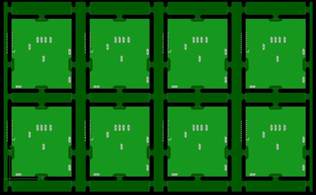
1. Panel Size and Layout Planning
Choosing the right panel size is critical. Most manufacturers have standard panel sizes, often ranging from 9x12 inches to 18x24 inches, though smaller options are available for hobbyists. Check your manufacturer’s PCB panel size guide to avoid extra fees for custom sizes. For home projects, start with a smaller panel (like 9x12 inches) to keep costs low while fitting multiple designs.
When planning your layout, ensure there’s enough space between individual boards for separation methods (more on this below). A common spacing is 0.1 to 0.2 inches (2.5 to 5 mm) to allow for clean cuts without damaging components.
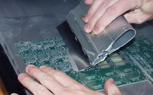
2. Separation Methods: V-Cuts and Mouse Bites
Once your panel is manufactured, the individual boards need to be separated. There are two beginner-friendly methods for this:
- V-Cuts: A V-shaped groove is cut into the panel, making it easy to snap boards apart by hand. This is ideal for straight edges and costs less, often included in standard manufacturing fees. Ensure your board edges are at least 0.012 inches (0.3 mm) thick for V-cuts to work without cracking.
- Mouse Bites: Small perforated holes are drilled along the edges, similar to a stamp sheet. Boards can be broken apart with minimal force. This method works for irregular shapes but may leave rough edges, so plan for a 0.02-inch (0.5 mm) clearance from components.
For hobbyists, V-cuts are often the easiest and most cost-effective choice for simple rectangular designs.
3. Fiducial Marks and Tooling Holes
Fiducial marks are small reference points (usually copper dots) placed on the panel to help assembly machines align components accurately. For beginners, place at least three fiducial marks on the panel, ideally near the corners, with a diameter of 0.04 inches (1 mm) and a clearance of 0.08 inches (2 mm) from other features.
Tooling holes are non-plated holes used to secure the panel during manufacturing. Most manufacturers require 3 to 4 holes with a diameter of 0.125 inches (3.175 mm) placed near the panel edges. Confirm these specs with your service provider to avoid delays.
Step-by-Step Guide to Easy PCB Panel Design
Now that you understand the basics, let’s walk through creating your first panelized design. This process is tailored for efficient PCB layout for home projects and beginners on a budget.
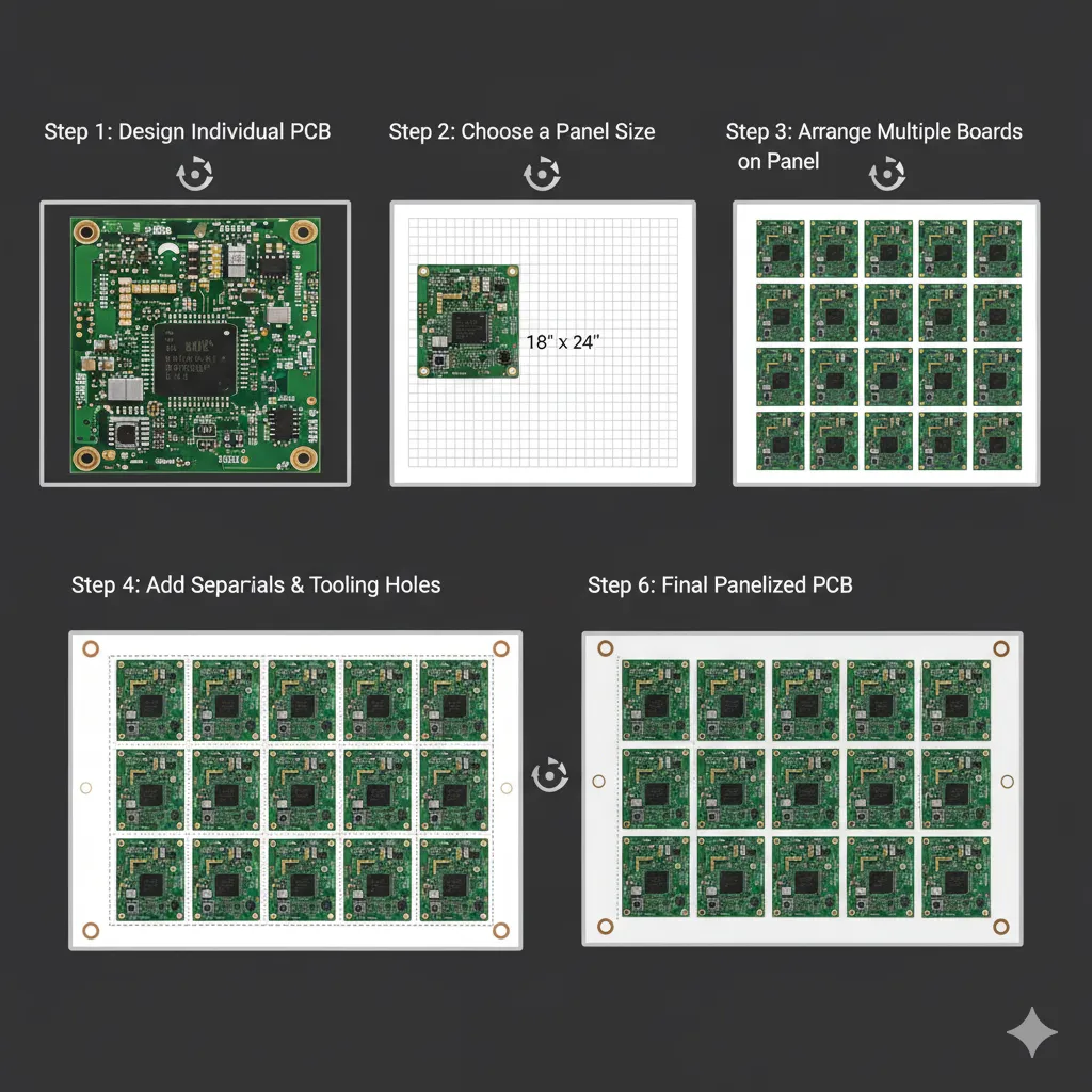
Step 1: Design Your Individual PCB
Start by designing your single PCB using software like KiCad or Eagle, both of which are free and beginner-friendly. Ensure your board dimensions are precise and leave a margin (at least 0.1 inches or 2.5 mm) around the edges for panelization spacing.
Step 2: Choose a Panel Size
Refer to your manufacturer’s guidelines for supported panel sizes. For hobby projects, a 10x10 inch panel often balances cost and capacity, fitting multiple small boards (e.g., 2x2 inches) with room for spacing.
Step 3: Arrange Multiple Boards on the Panel
Use your design software to duplicate and arrange your PCB layout on the panel. Align boards in a grid pattern for simplicity, ensuring consistent spacing (0.1 to 0.2 inches or 2.5 to 5 mm) between them for V-cuts or mouse bites.
Step 4: Add Separation Features
Mark the areas between boards for V-cuts or mouse bites in your design files. Most software allows you to draw cut lines or add perforation patterns. Double-check that no components or traces are too close to these lines to prevent damage during separation.
Step 5: Include Fiducials and Tooling Holes
Add fiducial marks and tooling holes as described earlier. These small additions can prevent costly assembly errors, especially for beginners new to automated manufacturing.
Free PCB Panelization Tools for Beginners
You don’t need expensive software to start panelizing. Here are some free PCB panelization tools that are perfect for hobbyists and beginners:
- KiCad: A free, open-source tool with built-in features to create panel layouts. Use the “Footprint Editor” to arrange multiple boards and add separation lines.
- FreeCAD: While primarily for mechanical design, it can be adapted for PCB panel layouts by importing board outlines and arranging them manually.
- GerbView: A free Gerber file viewer that lets you check and adjust panelized designs before sending them to manufacturing.
These tools are accessible and offer tutorials online, making them ideal for anyone starting with PCB panels for hobby projects.
Cost-Effective PCB Manufacturing Tips for Panelized Designs
Panelization is already a money-saver, but let’s explore additional ways to achieve cost-effective PCB manufacturing as a beginner.
1. Stick to Standard Specifications
Custom panel sizes, unusual board thicknesses (outside 1.6 mm standard), or special materials can increase costs by 20-50%. Stick to standard options offered by manufacturers to keep prices low.
2. Optimize Board Count per Panel
Maximize the number of boards on your panel without overcrowding. For example, a 10x10 inch panel can often fit 16 boards of 2x2 inches with proper spacing, reducing the per-unit cost significantly.
3. Order in Bulk
Many services offer discounts for larger quantities. Ordering a panel with 10-20 boards might cost less per board than ordering just 2-3 individual ones. Check pricing tiers before finalizing your order.
4. Avoid Over-Engineering
For hobby projects, you don’t need advanced features like gold plating or high-frequency materials unless your design demands it. A standard FR-4 material with 1 oz copper thickness is often sufficient and affordable.
Solder Paste Stencil for Beginners: Why It Matters in Panelization
If your panelized design includes surface-mount components, a solder paste stencil for beginners is a vital tool. A stencil is a thin sheet (often stainless steel) with cutouts matching your PCB’s pads. It helps apply solder paste evenly before placing components, ensuring clean soldering—especially important for panels with multiple boards.
For panelized designs, order a single stencil covering the entire panel. This saves time compared to using individual stencils for each board. Most manufacturers can create a stencil from your Gerber files for a small fee (around $5-10 for a small panel). Ensure the stencil thickness is 0.004 to 0.006 inches (0.1 to 0.15 mm) for standard applications, as thicker stencils can lead to excess paste and messy joints.
Common Mistakes to Avoid in Beginner PCB Panelization
As a beginner, it’s easy to make small errors that can lead to delays or extra costs. Here are pitfalls to watch out for:
- Insufficient Spacing: Placing boards too close together (less than 0.1 inches or 2.5 mm apart) can cause damage during separation. Always double-check spacing.
- Ignoring Manufacturer Guidelines: Each service has specific panelization rules. Failing to follow them can result in rejected designs or additional fees.
- Forgetting Fiducials: Without fiducial marks, assembly machines may misalign components, leading to costly rework.
- Overcomplicating Designs: For hobby projects, keep panel layouts simple. Complex arrangements with mixed designs can confuse manufacturers and increase costs.
Scaling Up: From Hobby Projects to Small Batches
Once you’re comfortable with PCB panels for hobby projects, panelization can help you transition to small-batch production. Start by designing larger panels (e.g., 12x18 inches) to fit more boards, and consider sharing panel space with other hobbyists to split costs. Many online communities offer “panel sharing” opportunities, reducing expenses further.
Additionally, use panelization to test multiple versions of a design on the same panel. For instance, place two slightly different layouts (e.g., with varied trace widths of 0.01 inches vs. 0.015 inches for signal integrity testing) on one panel to compare performance without extra manufacturing runs.
Final Thoughts on Maximizing Space on a Budget
PCB panelization is a powerful technique for beginners and hobbyists looking to save money and streamline production. By mastering beginner PCB panelization and following tips for easy PCB panel design, you can create efficient PCB layouts for home projects without breaking the bank. Use free tools, stick to standard sizes, and leverage panelization to get the most out of every manufacturing run. With a little planning, you’ll turn small ideas into big results while keeping costs low.
Whether you’re crafting a simple circuit at home or preparing for a small batch, panelization is your ticket to smarter, more cost-effective PCB manufacturing. Start small, experiment with layouts, and watch your skills—and savings—grow.


