 ALLPCB


Designing printed circuit boards (PCBs) for manufacturability (DFM) is critical to ensuring high-quality results, especially during panelization. One of the biggest challenges in this process is PCB warpage and maintaining board flatness panelization. Warpage can lead to assembly issues, component misalignment, and even board failure during high-temperature processes like reflow soldering. In this comprehensive guide, we’ll explore how DFM principles applied to PCB panelization can mitigate warpage, improve panel stiffness, and ensure flatness. From material selection warpage considerations to stress relief panelization techniques and support during reflow, we’ve got you covered with practical tips and insights.
What is PCB Panelization and Why Does Warpage Matter?
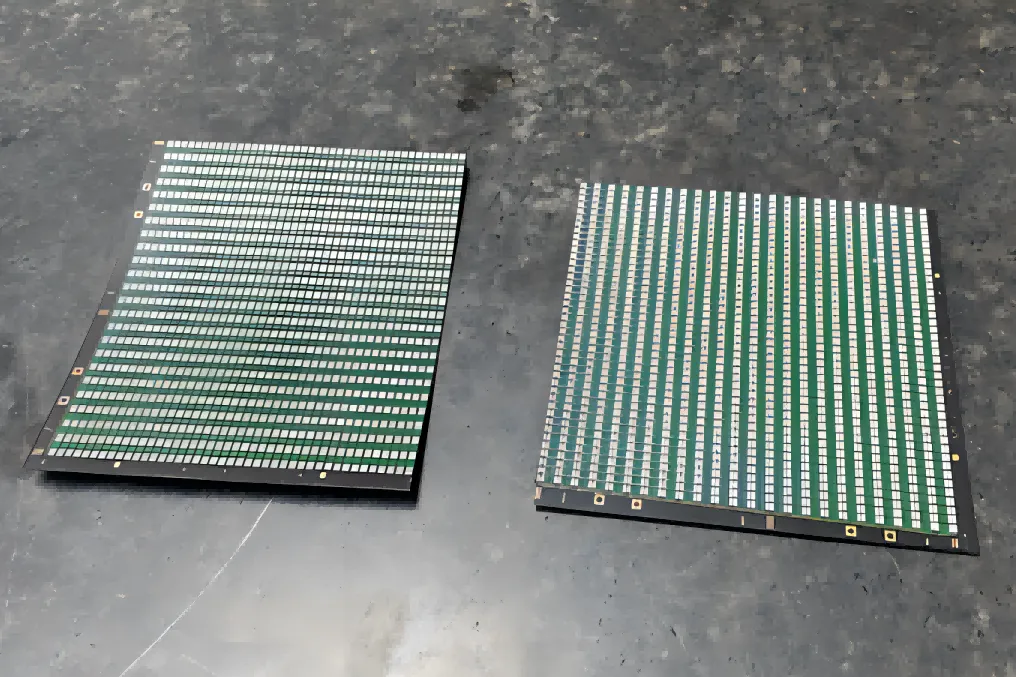
PCB panelization is the process of grouping multiple individual PCB designs into a single larger panel for manufacturing. This approach boosts efficiency, reduces costs, and simplifies handling during production. However, when panels are subjected to heat, mechanical stress, or improper design, warpage can occur. Warpage is the unwanted bending or twisting of the PCB, often caused by uneven thermal expansion, imbalanced copper distribution, or poor panel stiffness. According to industry standards like IPC, warpage should ideally be kept below 0.75% to avoid issues during assembly.
Warped boards can cause significant problems, such as misalignment of components during high-temperature assembly, soldering defects, or even complete failure of the board in extreme cases. By incorporating DFM strategies into panelization, manufacturers can minimize these risks and ensure consistent quality.
Key DFM Strategies for Mitigating PCB Warpage in Panelization
Let’s dive into specific DFM techniques that can help reduce warpage and maintain board flatness panelization. These strategies focus on design, material choices, and process optimization to address common causes of deformation.
1. Optimize Material Selection to Prevent Warpage
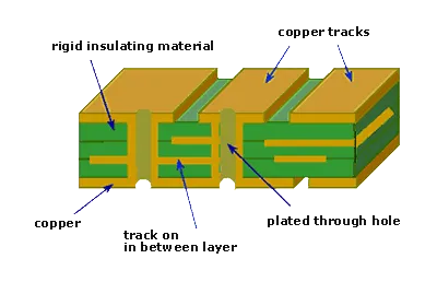
The choice of materials plays a huge role in controlling material selection warpage. Different materials have varying coefficients of thermal expansion (CTE), which determine how much they expand or contract under heat. Mismatched CTEs between the PCB substrate and copper layers can lead to stress and warpage during high-temperature assembly.
- Choose Low-CTE Materials: Opt for substrates like high-Tg FR-4 or polyimide for applications involving high temperatures. High-Tg materials can withstand temperatures up to 170°C or more without deforming, compared to standard FR-4, which may soften at 130°C.
- Balance Copper Distribution: Uneven copper distribution across layers can cause thermal imbalances. Ensure that copper coverage is as symmetrical as possible on both sides of the board. For instance, if one layer has 70% copper coverage, aim for a similar percentage on the opposite layer.
- Consider Thickness: Thicker boards (e.g., 1.6mm or above) generally offer better resistance to warpage due to increased rigidity. However, balance this with cost and weight considerations.
By carefully selecting materials and balancing their properties, you can significantly reduce the risk of warpage in large panels.
2. Enhance Panel Stiffness with Design Features
Achieving optimal panel stiffness is essential for maintaining flatness during manufacturing and assembly. Weak or poorly designed panels are more prone to bending under thermal or mechanical stress. Here are some design tips to improve stiffness:
- Add Breakaway Rails: Incorporate breakaway rail structures around the edges of the panel. These rails, often 5-10mm wide, provide additional support and rigidity during handling and soldering. They can be easily removed after assembly using scoring or mouse bites.
- Use Tooling Strips: Include non-functional areas or strips along the panel edges with tooling holes. These strips add structural integrity and help secure the panel during manufacturing processes.
- Distribute Boards Evenly: Arrange individual PCBs within the panel symmetrically to avoid stress concentration in specific areas. For example, avoid clustering all boards on one side of the panel, as this can lead to uneven weight distribution and bending.
These features not only enhance panel stiffness but also provide support during reflow, reducing the chances of deformation.
3. Implement Stress Relief Techniques in Panelization
Thermal and mechanical stresses are major contributors to warpage, especially during processes like reflow soldering. Applying stress relief panelization techniques can help manage these forces effectively.
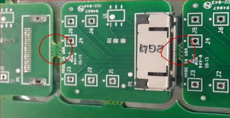
- V-Scoring and Tab Routing: Use V-scoring or tab routing to create separation lines between individual boards in the panel. These methods reduce stress by allowing slight flexibility during thermal expansion. V-scoring, for instance, creates a groove that weakens the material just enough for easy separation without compromising overall strength.
- Avoid Over-Constraining: Ensure that the panel design does not overly constrain the boards during heating and cooling cycles. Leave small gaps or use perforated tabs to allow for natural expansion and contraction.
- Thermal Relief Pads: For components with large thermal mass (like power ICs), use thermal relief pads in the design. These pads reduce heat transfer to surrounding areas, minimizing localized stress. A typical thermal relief pad might reduce heat dissipation by up to 30% compared to a solid pad.
By incorporating these stress relief panelization methods, you can keep internal stresses in check and maintain board flatness panelization.
4. Provide Support During Reflow Soldering
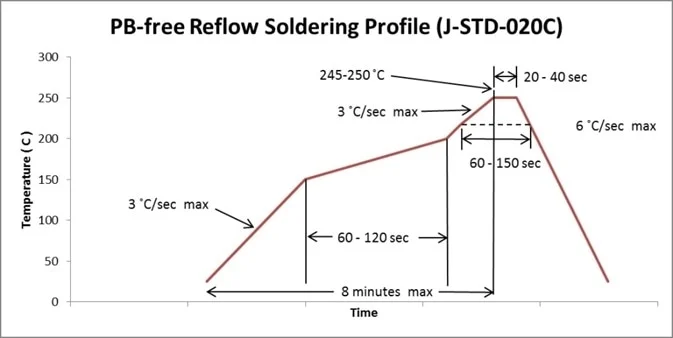
Reflow soldering, a critical step in PCB assembly, subjects panels to high temperatures (often exceeding 200°C). Without proper support during reflow, panels can sag or warp due to uneven heating. Here’s how to mitigate this:
- Use Support Fixtures: Design custom jigs or fixtures to hold the panel flat during the reflow process. These fixtures should match the panel’s dimensions and provide even support across the surface.
- Optimize Reflow Profiles: Adjust the reflow oven’s temperature profile to minimize thermal shock. Gradual heating and cooling ramps (e.g., 1-2°C per second) can reduce stress compared to rapid changes (3°C or more per second).
- Balance Component Placement: Avoid placing heavy or heat-intensive components on one side of the panel. Distribute them evenly to prevent localized hotspots that could cause bending.
Proper support during reflow ensures that the panel remains flat even under intense heat, preserving board flatness panelization.
5. Control Warpage in High-Temperature Assembly
High-temperature assembly processes, such as wave soldering or multiple reflow cycles, can exacerbate warpage if not managed properly. Here are some DFM tips to keep things under control:
- Minimize Reflow Cycles: If possible, limit the number of reflow cycles a panel undergoes. Each cycle increases the cumulative thermal stress on the board. For double-sided assembly, consider selective soldering for the second side to avoid a full reflow.
- Use Pre-Baking: Pre-bake the panel at a low temperature (around 120°C for 2-4 hours) before assembly to remove moisture. Moisture trapped in the board can vaporize during high-temperature assembly, leading to delamination or warpage.
- Monitor Panel Size: Larger panels (e.g., over 500mm in length) are more susceptible to warpage due to their size. If large panels are unavoidable, reinforce them with additional breakaway rail structures or split the design into smaller sub-panels.
By addressing these factors, you can significantly reduce the risk of deformation during high-temperature assembly.
Benefits of Applying DFM in PCB Panelization
Implementing DFM principles in panelization offers several advantages beyond just mitigating PCB warpage. These include:
- Improved Yield Rates: Flat, warp-free panels lead to fewer assembly errors, increasing overall production yield. A reduction in warpage from 1.5% to 0.5% can improve yield by as much as 10% in high-volume production.
- Cost Savings: Reducing defects and rework saves time and materials. For instance, avoiding a single failed panel can save hundreds of dollars in large-scale manufacturing.
- Better Reliability: Boards with proper board flatness panelization ensure reliable soldering and component placement, leading to longer-lasting products.
- Faster Time-to-Market: Streamlined manufacturing processes mean quicker turnaround times, helping you meet tight deadlines without compromising quality.
Common Mistakes to Avoid in PCB Panelization
Even with the best intentions, certain oversights can lead to warpage and flatness issues. Here are some pitfalls to steer clear of:
- Ignoring Copper Balance: Failing to balance copper across layers can create uneven thermal expansion, leading to warpage. Always double-check layer symmetry during design reviews.
- Overloading Panels: Packing too many boards into a single panel without adequate spacing or support can weaken panel stiffness and increase stress.
- Skipping Thermal Analysis: Not simulating thermal behavior before production can result in unexpected warpage during high-temperature assembly. Use simulation tools to predict and address potential issues.
Conclusion: Achieving Flatness and Quality Through DFM
Mitigating PCB warpage and ensuring board flatness panelization are achievable goals when DFM principles are applied to PCB panelization. By focusing on material selection warpage considerations, enhancing panel stiffness with features like breakaway rail structures, and providing support during reflow, you can minimize deformation and improve manufacturing outcomes. Techniques like stress relief panelization and careful management of high-temperature assembly further contribute to success.
At ALLPCB, we’re committed to helping you navigate these challenges with expert guidance and cutting-edge solutions. By incorporating these DFM strategies into your design and manufacturing process, you’ll achieve flatter boards, higher yields, and more reliable products. Start optimizing your panelization today for better results tomorrow!


