ALLPCB


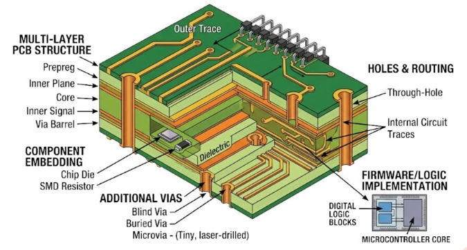
Blind vias are a crucial element in modern printed circuit board (PCB) design, especially for high-density interconnect (HDI) applications. If you're looking to understand blind via laser drilling and how to master techniques like laser drilling depth control, you're in the right place. This blog dives deep into the world of PCB blind vias and microvia drilling techniques, offering practical insights for engineers and designers aiming to optimize their PCB manufacturing processes.
At its core, blind via creation using laser drilling is about precision and efficiency. This technology allows for smaller, more accurate vias that connect outer layers to inner layers without passing through the entire board. Below, we'll explore the intricacies of this process, from the basics of blind vias to advanced depth control methods, ensuring your designs meet the highest standards of performance and reliability.
What Are Blind Vias and Why Do They Matter in PCB Design?
Blind vias are vertical interconnects in a PCB that connect an outer layer to one or more inner layers without extending through the entire board. Unlike through-hole vias, which go all the way through, blind vias save space and improve signal integrity, making them ideal for compact, high-speed designs.
In today's electronics, where devices are shrinking while performance demands grow, blind vias are essential. They allow for denser component placement and shorter signal paths, reducing impedance and enhancing circuit reliability. For instance, in HDI boards used in smartphones or medical devices, blind vias can help achieve impedance values as low as 50 ohms for high-speed signals, ensuring minimal signal loss.
The primary method for creating these vias is laser drilling, which offers unmatched precision compared to traditional mechanical drilling. Let’s break down how this technology works and why it’s a game-changer for PCB blind vias.
Understanding Laser Drilling for Blind Vias
Laser drilling is a non-contact process that uses focused laser beams to create microvias and blind vias in PCBs. This technique is particularly effective for HDI designs, where via sizes often range from 50 to 150 micrometers in diameter. The precision of laser drilling ensures that these tiny holes are placed accurately without damaging surrounding materials.
There are two main types of lasers used in this process: CO2 lasers and Nd:YAG lasers. CO2 lasers are often preferred for drilling through dielectric materials because they stop naturally at the copper layer beneath, preventing damage. Nd:YAG lasers, on the other hand, are used for trepanning or cutting through the top copper layer before the dielectric is removed. This two-step process ensures clean, precise blind vias with minimal thermal impact.
The benefits of blind via laser drilling are clear: it allows for smaller via sizes, reduces the risk of board damage, and supports high-volume manufacturing. However, achieving consistent results requires careful control over various parameters, especially depth.
The Importance of Laser Drilling Depth Control
One of the biggest challenges in creating blind vias is maintaining precise depth. If the laser drills too deep, it can damage underlying layers or create unwanted connections. If it’s too shallow, the via may not connect properly, leading to electrical failures. This is where laser drilling depth control becomes critical.
Depth control in laser drilling relies on several factors:
- Laser Pulse Energy: Adjusting the energy of the laser pulse can determine how much material is removed per shot. Lower energy settings allow for finer control, especially for thin dielectric layers (e.g., 50-100 micrometers).
- Pulse Duration: Using ultrashort pulses, such as those in the picosecond or femtosecond range, minimizes heat buildup and ensures cleaner cuts with precise depth.
- Material Properties: Different PCB materials, like FR-4 or high-frequency laminates, absorb laser energy differently. Calibration based on material thickness and type is essential.
- Feedback Systems: Modern laser drilling machines often include real-time monitoring systems that adjust parameters on the fly to maintain consistent depth.
For example, when drilling a blind via to connect layer 1 to layer 2 in a multilayer PCB, the target depth might be around 100 micrometers. A deviation of even 10 micrometers can lead to signal integrity issues, especially in high-frequency applications where signal speeds exceed 5 GHz. Precision in laser drilling depth control is non-negotiable for reliable performance.
Key Microvia Drilling Techniques for Optimal Results
Microvias, which include blind and buried vias, are the backbone of HDI PCB designs. Mastering microvia drilling techniques can significantly enhance your board’s performance. Here are some proven methods used in the industry:
1. Trepanning for Copper Removal
Trepanning involves using a laser to cut a circular path through the top copper layer before drilling into the dielectric material. This technique, often performed with an Nd:YAG laser, ensures a clean entry point for the via and prevents copper burrs that could affect electrical performance.
2. Percussion Drilling for Dielectric Layers
Percussion drilling uses rapid, high-energy laser pulses to remove dielectric material layer by layer. This method is ideal for creating blind vias with diameters as small as 50 micrometers, ensuring minimal heat-affected zones and smooth via walls.
3. Helical Drilling for Precision
Helical drilling moves the laser in a spiral pattern to create vias with exceptional sidewall quality. This technique is slower but offers superior precision, making it suitable for critical applications where signal integrity is paramount.
Each of these microvia drilling techniques has its place depending on the design requirements. For high-speed digital circuits, where signal reflection must be minimized, helical drilling might be the best choice. For cost-sensitive projects with less stringent requirements, percussion drilling offers a faster, more economical solution.
Challenges in Blind Via Laser Drilling and How to Overcome Them
While laser drilling offers many advantages, it’s not without challenges. Addressing these issues head-on can ensure consistent quality in your PCB production.
Thermal Damage
Excessive heat from the laser can cause charring or delamination of the PCB material, especially in thin or sensitive laminates. Using ultrashort pulse lasers and optimizing energy settings can minimize thermal impact. For instance, femtosecond lasers reduce heat buildup by delivering energy in bursts shorter than 10^-15 seconds.
Via Wall Quality
Rough or uneven via walls can lead to poor plating and unreliable connections. Techniques like helical drilling and post-drilling cleaning processes (e.g., desmearing with plasma or chemical solutions) can improve wall smoothness, ensuring better conductivity.
Depth Consistency Across Large Batches
In high-volume manufacturing, maintaining consistent depth across thousands of vias is a challenge. Automated systems with real-time feedback and calibration for material variations can help achieve uniformity. Regular maintenance of laser equipment also plays a vital role in sustaining precision.
By focusing on these solutions, manufacturers can overcome the hurdles of blind via laser drilling and produce boards that meet the tight tolerances of modern electronics.
Benefits of Laser-Drilled Blind Vias in HDI Designs
The shift to laser-drilled blind vias has transformed PCB design, especially for HDI applications. Here are some key advantages that make this technology indispensable:
- Space Efficiency: Blind vias allow for tighter component spacing, reducing board size by up to 30% in some designs.
- Improved Signal Integrity: Shorter signal paths minimize impedance mismatches, supporting high-speed signals above 10 GHz with minimal loss.
- Enhanced Reliability: Precise drilling reduces the risk of defects, leading to more durable boards that withstand harsh operating conditions.
- Cost-Effective for Complex Designs: While laser drilling equipment is an investment, it reduces the need for multiple drilling passes and rework, saving time and resources in the long run.
These benefits highlight why mastering PCB blind vias through laser drilling is a priority for engineers working on cutting-edge technology.
Best Practices for Implementing Laser Drilling in PCB Production
To get the most out of laser drilling for blind vias, consider these best practices:
- Material Selection: Choose PCB materials with consistent thickness and laser absorption properties to ensure uniform drilling results.
- Design Optimization: Work closely with your design software to place vias strategically, avoiding areas with dense copper traces that could interfere with laser focus.
- Equipment Calibration: Regularly calibrate laser systems to maintain accuracy in depth and diameter, especially for vias smaller than 100 micrometers.
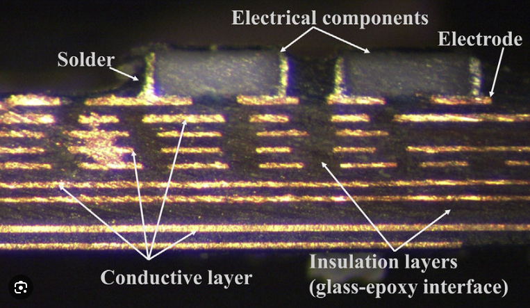
- Quality Inspection: Use automated optical inspection (AOI) and cross-section analysis to verify via quality after drilling, ensuring no defects go unnoticed.
Following these steps can streamline your production process and deliver high-quality boards that meet the demands of modern applications.
Future Trends in Blind Via Laser Drilling
As technology evolves, so does the field of laser drilling for PCBs. Emerging trends include the use of even shorter pulse lasers for reduced thermal impact and the integration of artificial intelligence for real-time process optimization. These advancements promise to push the boundaries of what’s possible with microvia drilling techniques, enabling even smaller, more complex designs.
Additionally, the demand for eco-friendly manufacturing is driving research into laser systems that consume less energy while maintaining high precision. Staying ahead of these trends can give manufacturers a competitive edge in producing next-generation electronics.
Conclusion: Elevating PCB Design with Laser-Drilled Blind Vias
Mastering the art of blind via creation through laser drilling is a powerful way to elevate your PCB designs. From achieving precise laser drilling depth control to leveraging advanced microvia drilling techniques, this technology offers unmatched benefits for HDI applications. By understanding the nuances of blind via laser drilling and implementing best practices, you can create compact, reliable, and high-performing boards that meet the needs of today’s fast-paced electronics industry.
Whether you're working on consumer gadgets, automotive systems, or medical devices, the precision and efficiency of laser-drilled PCB blind vias can make all the difference. Embrace these techniques to stay at the forefront of PCB innovation and deliver products that stand out in quality and performance.