If you're looking for a clear guide on PCB panelization design rules, you've come to the right place. PCB panelization is the process of grouping multiple printed circuit boards (PCBs) onto a single panel for efficient manufacturing. Following proper design guidelines ensures cost savings, smoother production, and high-quality results. In this comprehensive checklist, we'll cover essential aspects like PCB panel spacing, border requirements, tooling holes, and general design tips for manufacturing.
Whether you're a seasoned engineer or just starting out, this blog will walk you through every detail of PCB panelization design. Let's dive into the rules and best practices to optimize your PCB designs for production.
What is PCB Panelization and Why Does It Matter?
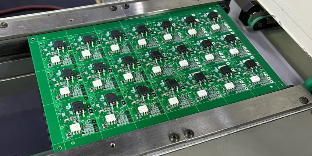
PCB panelization is a technique used in manufacturing where multiple smaller PCBs are arranged on a larger panel. This approach streamlines the production process, reduces material waste, and lowers costs by allowing manufacturers to handle several boards at once. It also simplifies automated assembly processes, such as pick-and-place operations, by providing a uniform layout.
Without proper panelization, you risk delays, increased costs, or even damaged boards during production. Following design rules for panelization ensures that your boards are compatible with manufacturing equipment, easy to separate after production, and free from errors. Let’s explore the key guidelines to achieve this.
Key PCB Panelization Design Guidelines
To create an effective panel design, you need to follow specific rules that align with manufacturing capabilities. Below is a detailed checklist covering the most critical aspects of PCB panelization design guidelines.
1. PCB Panel Spacing: Ensure Proper Gaps Between Boards
Spacing between individual PCBs on a panel is crucial for manufacturing and depanelization (separating the boards after production). Insufficient spacing can lead to damage during cutting or assembly, while excessive spacing wastes valuable panel space.
- Minimum Spacing: Maintain at least 2-3 mm of spacing between individual boards. This allows enough room for cutting tools like routers or V-scoring blades to separate the boards without damaging components or traces.
- Component Clearance: If components are placed near the edges of a board, increase the spacing to 5 mm or more to prevent damage during depanelization.
- Edge-to-Edge Uniformity: Keep spacing consistent across the panel to ensure uniform stress distribution during manufacturing processes.
By adhering to these spacing rules, you reduce the risk of errors and improve the efficiency of the production line.
2. PCB Panel Border Requirements: Define Clear Margins
The border, or frame, around the panel is an essential part of the design. It provides structural support during manufacturing and space for tooling holes and fiducials (alignment markers). Neglecting border requirements can result in panels that are difficult to handle or incompatible with assembly equipment.
- Border Width: Allocate a border width of at least 5-10 mm around the entire panel. This margin ensures there’s enough room for handling and mounting without interfering with the PCBs.
- No Components in Border: Keep the border free of components, traces, or vias. This area is reserved for manufacturing aids like tooling holes and test points.
- Panel Edge Clearance: Ensure that no board edges are closer than 5 mm to the panel’s outer edge to avoid stress fractures during handling.
Proper border design not only supports manufacturing but also protects your boards from damage during transport and processing.
3. PCB Panel Tooling Holes: Support Accurate Alignment
Tooling holes are small, non-plated holes placed in the panel border to help align the panel during manufacturing. They ensure precise registration for drilling, routing, and assembly processes. Without properly placed tooling holes, alignment errors can occur, leading to defective boards.
- Hole Size: Use a diameter of 2-3 mm for tooling holes, as this size is compatible with most manufacturing equipment.
- Placement: Position at least three tooling holes in the border, ideally in a triangular pattern (e.g., one in each corner except one to avoid symmetry issues). Place them at least 5 mm away from the panel edge.
- Non-Plated Design: Ensure tooling holes are non-plated to avoid electrical interference and reduce production costs.
Tooling holes are a small but critical detail in PCB design for manufacturing. They help maintain precision throughout the production process.
4. Breakaway Tabs and V-Scoring: Simplify Depanelization
Depanelization is the process of separating individual PCBs from the panel after manufacturing. Two common methods are breakaway tabs (also called mouse bites) and V-scoring. Designing these features correctly prevents damage to boards during separation.
- Breakaway Tabs: Use small perforated tabs to connect individual boards to the panel or to each other. Place 3-5 tabs per board, each with a width of 4-6 mm and holes of 0.5 mm diameter for easy breaking. Position tabs away from sensitive components or traces.
- V-Scoring: For straight edges, use V-shaped grooves cut into the panel (typically at a 30-45-degree angle). Ensure a minimum residual thickness of 0.3-0.5 mm to maintain panel strength during handling but allow easy separation.
- Clearance from Components: Keep tabs and scoring lines at least 2 mm away from components to avoid stress or damage during depanelization.
Choosing the right depanelization method and designing it properly ensures that your boards can be separated cleanly and without defects.
5. Fiducial Marks: Enhance Assembly Precision
Fiducial marks are small reference points on the panel used by automated assembly machines to align components accurately. They are essential for high-precision processes like surface-mount technology (SMT).
- Size and Shape: Design fiducials as circular marks with a diameter of 1-1.5 mm, surrounded by a clear area (no solder mask) of at least 2 mm.
- Placement: Place at least three fiducials on the panel border in a non-symmetrical pattern to avoid alignment confusion. Additionally, include fiducials on individual boards if space allows.
- Material: Use bare copper for fiducials to ensure visibility for optical recognition systems.
Including fiducial marks in your panel design minimizes assembly errors and improves the overall quality of the finished product.
6. Panel Size and Material Utilization: Optimize for Cost
The size of your panel and how you arrange the boards on it directly impact manufacturing costs. Larger panels can accommodate more boards, reducing waste, but they must fit within the manufacturer’s equipment limits.
- Standard Panel Sizes: Common panel sizes include 18x24 inches or 9x12 inches. Check with your manufacturer for their preferred dimensions to avoid additional setup fees.
- Board Orientation: Arrange boards to maximize the number per panel while maintaining required spacing and border widths. Rotate boards if necessary to fit more efficiently.
- Material Waste: Aim to use at least 70-80% of the panel area for actual PCBs to keep costs down. Empty spaces increase material costs without adding value.
Optimizing panel size and layout is a practical way to balance production efficiency with cost savings.
Additional PCB Design for Manufacturing Tips
Beyond panelization-specific rules, there are general PCB design practices that enhance manufacturability. Incorporating these into your workflow ensures a smoother production process.
- Component Placement: Avoid placing components too close to board edges (maintain at least 3 mm clearance) to prevent damage during depanelization or handling.
- Trace Routing: Keep traces at least 0.2 mm away from board edges to avoid exposure or damage during cutting. Use a minimum trace width of 0.15 mm for standard designs to ensure reliability.
- Panel Strength: For thin boards (less than 1.6 mm thick), add extra border width or support tabs to prevent warping during manufacturing.
These manufacturing-friendly design choices complement panelization rules and contribute to a high-quality final product.
Common Mistakes to Avoid in PCB Panelization
Even with a solid checklist, mistakes can happen. Here are some common pitfalls to watch out for when designing your PCB panel:
- Ignoring Manufacturer Guidelines: Every manufacturer has specific panelization requirements. Failing to follow them can lead to delays or additional costs. Always request and review their design rules before finalizing your layout.
- Overcrowding the Panel: Trying to fit too many boards without proper spacing risks damage and reduces yield. Stick to the recommended gaps and border widths.
- Misplaced Tooling Holes or Fiducials: Incorrect placement can cause alignment issues, leading to assembly errors. Double-check their positions in the border area.
- Inadequate Depanelization Design: Weak tabs or poorly planned V-scoring can make separation difficult or damage boards. Test your design with a prototype if possible.
Avoiding these errors will save you time, money, and frustration during the manufacturing process.
Conclusion: Master PCB Panelization for Better Results
PCB panelization is a vital step in optimizing your design for manufacturing. By following this comprehensive checklist, you can ensure proper PCB panel spacing, meet border requirements, place tooling holes accurately, and design for efficient depanelization. These guidelines not only improve production efficiency but also reduce costs and enhance the quality of your finished boards.
Remember to consider every detail, from spacing and borders to fiducials and material utilization. A well-designed panel is the foundation of a successful PCB project. Use these PCB panelization design guidelines as your go-to resource, and you'll be well on your way to creating manufacturing-ready designs that deliver outstanding results.
 ALLPCB


