In the rapidly growing field of renewable energy, solar power inverters play a critical role in converting solar energy into usable electricity. At the heart of these inverters lies a key component: the printed circuit board (PCB). Specifically, heavy copper PCBs are becoming increasingly important due to their ability to handle high currents and manage heat effectively. If you're wondering how heavy copper PCBs contribute to solar inverter performance, the answer is simple—they provide durability, improved thermal management, and support for high current loads, all of which are essential for efficient solar energy conversion.
In this blog, we'll dive deep into the significance of heavy copper PCBs in solar power inverters. We'll explore their unique features, why they are ideal for high current PCB design, and how PCB thickness for solar applications impacts performance. Whether you're an engineer designing solar systems or a business looking to understand the technology behind renewable energy, this guide will provide valuable insights into solar inverter PCB technology.
What Are Heavy Copper PCBs and Why Do They Matter?
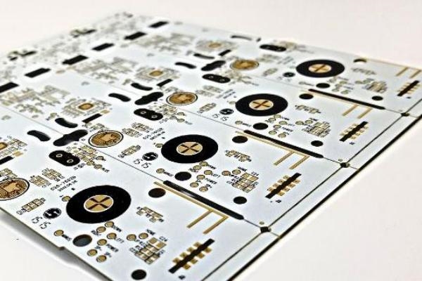
Heavy copper PCBs are specialized circuit boards that feature thicker copper layers compared to standard PCBs. While a typical PCB might have copper layers of 1 to 2 ounces per square foot (oz/ft2), heavy copper PCBs can have copper thicknesses ranging from 3 oz/ft2 up to 40 oz/ft2 or more. This increased thickness allows them to carry higher electrical currents and dissipate heat more effectively, making them ideal for power-intensive applications like solar power inverters.
In solar inverters, the primary function is to convert direct current (DC) from solar panels into alternating current (AC) for household or industrial use. This process involves handling significant power loads, often in the range of several kilowatts. A heavy copper PCB ensures that the inverter can manage these high currents without overheating or degrading over time, thus enhancing reliability and lifespan.
The Unique Demands of Solar Inverter PCBs
Solar power inverters operate under demanding conditions. They must handle fluctuating power levels, endure environmental stresses like heat and humidity, and maintain efficiency over long periods. These factors place specific requirements on the PCB design, especially in terms of current capacity and thermal management.
A typical solar inverter for residential use might handle currents ranging from 10 to 50 amps, while industrial inverters can exceed 100 amps. Standard PCBs with thin copper layers would struggle under such loads, leading to increased resistance, heat buildup, and potential failure. Heavy copper PCBs address this by reducing electrical resistance—often below 1 milliohm per trace—and improving heat dissipation, which can lower operating temperatures by 10-20°C compared to standard designs.
Additionally, solar inverter PCBs must be robust enough to withstand thermal cycling, where temperatures fluctuate between day and night or due to seasonal changes. Heavy copper construction adds mechanical strength, preventing cracks or delamination in the board over time.
Key Benefits of Heavy Copper PCBs in Solar Inverters
Let’s break down the specific advantages that heavy copper PCBs bring to solar power inverters. These benefits directly address the challenges of high current PCB design and ensure optimal performance.
1. Enhanced Current Carrying Capacity
The thicker copper layers in heavy copper PCBs allow them to carry much higher currents without overheating. For example, a 4 oz/ft2 copper layer can safely handle currents up to 20-30 amps per trace, depending on width, compared to just 5-10 amps for a 1 oz/ft2 layer. This is crucial for solar inverters, where power conversion generates significant electrical loads.
2. Superior Thermal Management
Heat is a major concern in solar inverters, as excessive temperatures can reduce efficiency and damage components. Heavy copper PCBs act as a heat sink, spreading thermal energy across the board and away from sensitive areas. Studies suggest that heavy copper designs can reduce hotspot temperatures by up to 15%, extending the lifespan of the inverter.
3. Increased Durability and Reliability
The robust construction of heavy copper PCBs makes them less prone to damage from thermal stress or mechanical shock. This durability is especially important for solar inverters installed in outdoor environments, where they may be exposed to harsh weather conditions.
4. Compact Design for High Power
By using heavy copper, designers can reduce the number of layers or board size while still meeting power requirements. This leads to more compact and cost-effective solar inverter designs without sacrificing performance.
PCB Thickness for Solar Applications: Why It Matters
PCB thickness for solar power inverters is a critical design parameter that goes hand-in-hand with heavy copper construction. Thickness affects not only the current capacity but also the thermal and mechanical properties of the board.
In heavy copper PCBs for solar inverters, copper thickness often ranges from 3 to 10 oz/ft2, depending on the power rating of the inverter. For a 5 kW residential inverter, a copper thickness of 4-6 oz/ft2 might suffice, while a 50 kW commercial inverter may require 8-10 oz/ft2 or more to handle higher currents. The overall board thickness, including substrate materials like FR4, typically falls between 1.6 mm and 3.2 mm to provide structural stability.
A thicker copper layer reduces electrical resistance, which can be quantified using the formula R = ρL/A, where R is resistance, ρ is the resistivity of copper (1.68 x 10^-8 Ω·m), L is the length of the trace, and A is the cross-sectional area. Doubling the copper thickness effectively halves the resistance, allowing for higher current flow with less heat generation.
However, increasing thickness must be balanced with cost and manufacturability. Thicker copper layers require specialized fabrication processes, such as selective plating or embedded copper techniques, to ensure uniform deposition and prevent defects. Engineers must carefully evaluate the trade-offs to optimize performance for specific solar inverter applications.
High Current PCB Design Considerations for Solar Inverters
Designing a high current PCB for solar inverters involves more than just using heavy copper. Several factors must be considered to ensure efficiency, safety, and reliability. Here are some key design principles:
1. Trace Width and Spacing
Wider traces are necessary to handle high currents, as they increase the cross-sectional area for current flow. For instance, a trace carrying 20 amps might need a width of 5-7 mm with 4 oz/ft2 copper to keep resistance low. Adequate spacing between traces is also essential to prevent arcing or short circuits, especially in high-voltage sections of the inverter.
2. Thermal Vias and Heat Sinks
Thermal vias—small holes filled with conductive material—help transfer heat from the copper layers to external heat sinks or the opposite side of the board. In solar inverter PCBs, placing thermal vias near high-power components like MOSFETs or IGBTs can reduce local temperatures by 5-10°C.
3. Material Selection
The substrate material must withstand high temperatures and provide good insulation. FR4 is commonly used for its cost-effectiveness, but high-performance materials like polyimide may be chosen for extreme conditions. The dielectric constant of the material (typically 4.2-4.5 for FR4) also affects signal integrity in control circuits.
4. Layer Stackup
A well-planned layer stackup is critical for high current PCB design. Power and ground planes should be placed close to each other to minimize loop inductance, which can be as low as 1-2 nH with proper design. This reduces electromagnetic interference (EMI) and improves inverter efficiency.
Challenges and Solutions in Using Heavy Copper PCBs
While heavy copper PCBs offer significant advantages, they also present unique challenges in manufacturing and design. Understanding these challenges helps engineers make informed decisions for solar inverter applications.
One challenge is the increased cost of fabrication. Producing heavy copper PCBs requires advanced equipment and longer etching times, which can raise costs by 20-30% compared to standard PCBs. However, this cost is often justified by the improved performance and reliability in high-power applications like solar inverters.
Another issue is the potential for uneven copper deposition during manufacturing, which can lead to weak spots or delamination. To address this, manufacturers use techniques like step plating or selective copper buildup to ensure uniform thickness across the board.
Finally, the added weight of heavy copper can impact the overall design of the inverter, especially in portable or space-constrained systems. Engineers can mitigate this by optimizing the board layout to use heavy copper only in high-current areas, combining it with standard copper in less demanding sections.
Future Trends: Heavy Copper PCBs in Renewable Energy
As the demand for renewable energy grows, so does the need for advanced PCB technologies. Heavy copper PCBs are poised to play an even larger role in the future of solar power inverters. Emerging trends include the integration of hybrid copper designs, where different copper thicknesses are used on the same board to balance cost and performance.
Additionally, advancements in materials science are leading to substrates with better thermal conductivity, allowing heavy copper PCBs to handle even higher power densities. For instance, ceramic-based substrates could reduce thermal resistance by up to 50%, enabling more compact and efficient solar inverters.
The push for higher efficiency in solar systems—often targeting above 98%—will also drive innovation in high current PCB design. Engineers are exploring multi-layer heavy copper configurations to support complex inverter topologies like three-phase systems, which are common in commercial and industrial applications.
Conclusion: Why Choose Heavy Copper PCBs for Solar Inverters?
Heavy copper PCBs are a game-changer for solar power inverters, offering unmatched performance in handling high currents, managing heat, and ensuring long-term reliability. Their thicker copper layers and robust construction make them ideal for the demanding conditions of solar energy conversion, from residential systems to large-scale industrial setups.
For engineers and businesses involved in solar technology, understanding the role of heavy copper PCBs is essential for designing efficient and durable inverters. By prioritizing high current PCB design and optimizing PCB thickness for solar applications, you can achieve better energy conversion, lower maintenance costs, and a stronger return on investment.
At ALLPCB, we specialize in providing cutting-edge solutions for solar inverter PCBs, including heavy copper designs tailored to your specific needs. Whether you're scaling up production or prototyping a new system, our expertise ensures that your solar projects are built on a solid foundation of quality and innovation.
 ALLPCB


