 ALLPCB


What is a PCB Burr?
A PCB burr is a small, unwanted piece of copper or board material left over after cutting or drilling. You can find them at several stages:
- Cutting Burrs: On the edges of the board after the main panel is cut.
- Drilling Burrs: Around the rim of newly drilled holes.
- Routing Burrs: Along the final outline of the board after it is shaped.
- V-Cut Burrs: On the edges where a board is snapped from a larger panel.
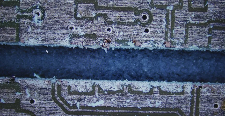
These small pieces of material can cause big problems. They can break off and create short circuits, stop components from sitting flat on the board, or block the copper plating inside holes, leading to a bad electrical connection.
Why Do Burrs Happen?
Burrs are not random. They are caused by specific issues in the manufacturing process:
- Dull Tools: A sharp tool cuts cleanly. A dull tool tears the material instead, creating rough, jagged edges.
- Wrong Machine Settings: If a drill or router moves too fast or pushes too hard, it rips the copper instead of cutting it smoothly.
- Complex Shapes: Sharp inside corners or complicated outlines can be difficult to cut cleanly, making them likely places for burrs to form.
- V-Cut Issues: The V-cut process, used to separate boards from a panel, needs to be very precise. The wrong angle or depth can easily create a rough, burred edge when the board is snapped off.
The Consequences: Why Burrs Are a Serious Problem
A PCB with burrs is not just a cosmetic issue; it's a direct threat to the function and reliability of the final product. Here are the most common problems burrs can cause:
- Electrical Shorts: This is the most dangerous risk. Burrs are small, loose pieces of conductive copper. During assembly, shipping, or even just from vibration, these pieces can break off and land between two pads or traces. This creates an unintended electrical connection, or a 'short circuit,' which can cause the device to malfunction immediately or even damage components permanently.
- Poor Soldering and Component Assembly: Burrs around component pads can prevent parts from sitting perfectly flat on the board. This is especially problematic for fine-pitch components with many small legs. An uneven surface can lead to poor solder joints, where some connections are weak or not connected at all. This results in a faulty assembly that is difficult to diagnose and repair.
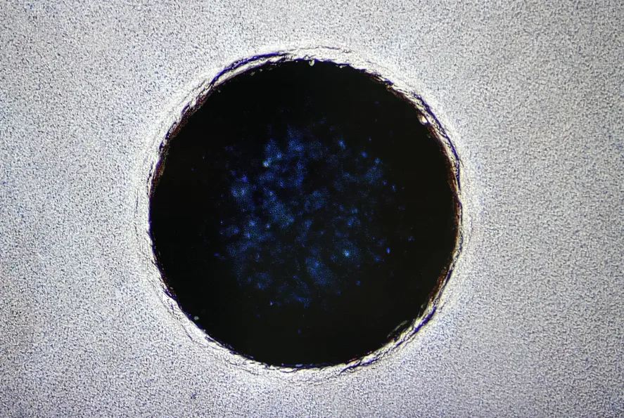
- Unreliable Connections Between Layers: Burrs around a drilled hole are particularly damaging. These holes (vias) are plated with copper to connect different layers of the PCB. A burr on the edge of the hole disrupts this plating process, causing the copper layer inside the hole to be thin, uneven, or incomplete. This creates a weak electrical connection that might work at first but can easily fail later under normal operating conditions.
- Long-Term Failure: A product might pass its initial tests, but a loose burr can become a ticking time bomb. Over time, heat and vibration can cause it to move and create a short circuit long after the product has been shipped to a customer. This leads to unexpected failures and damages a product's reputation for reliability.
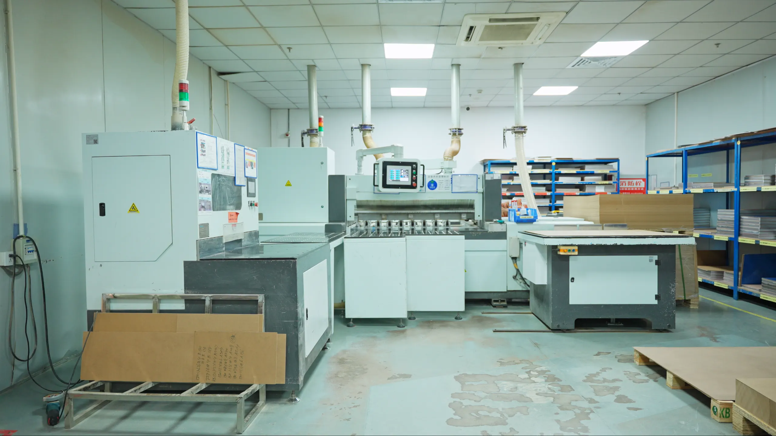
The ALLPCB Solution: A Detailed Look at Our Process
At ALLPCB, we focus on stopping burrs before they even start. We have built a careful, multi-step process to ensure every board is clean.
Stage 1: The First Cut (Material Preparation)
The fight against burrs starts with the raw material.
- High-Quality Equipment: We use industry-leading Leaway automatic cutting machines. These machines are known for making extremely precise and clean cuts from the very beginning.
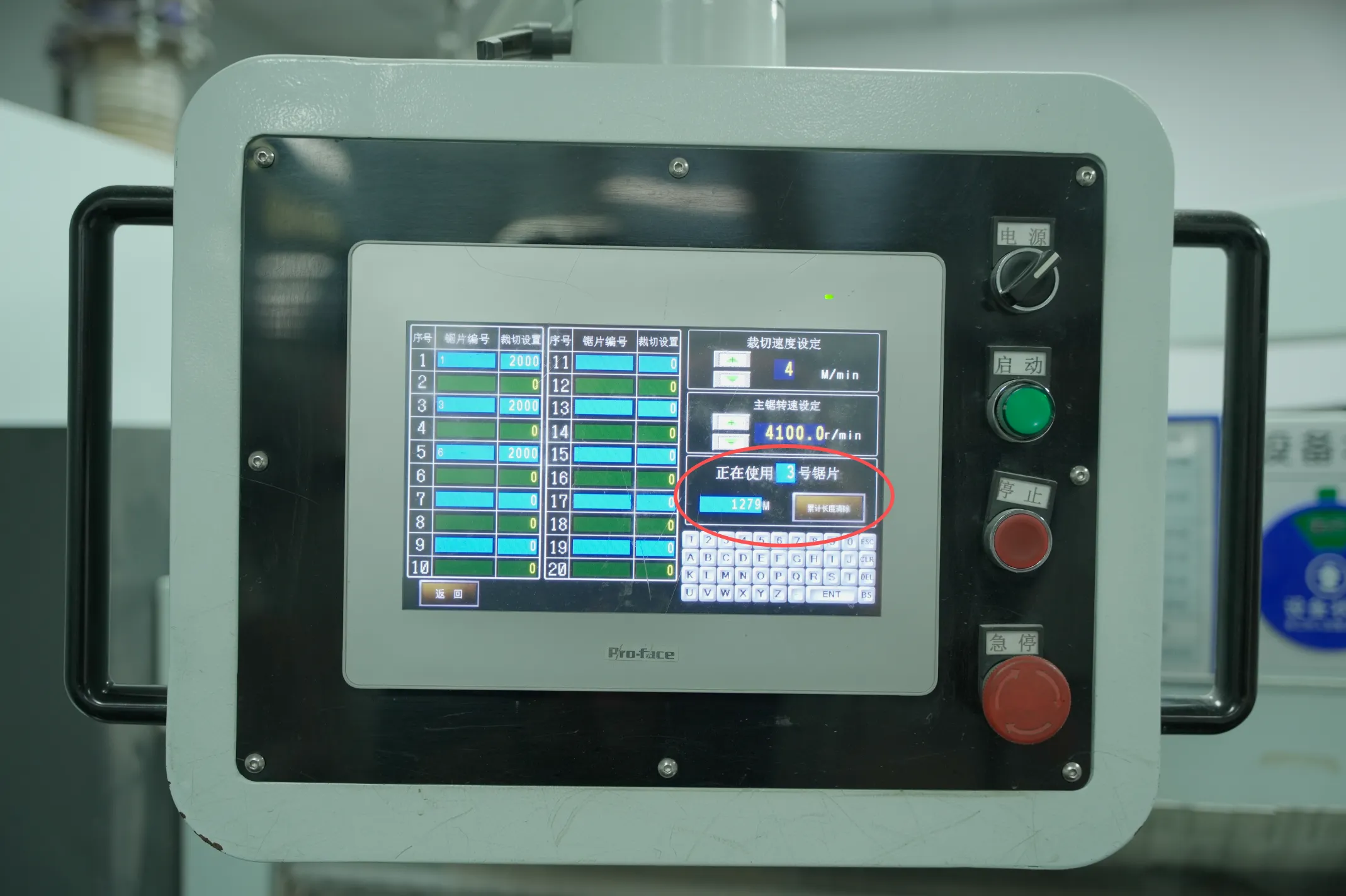
- Strict Tool Management: A sharp blade is key. We have a strict policy for our cutting tools: each blade is replaced after it has cut between 2000 and 2500 meters of material. If our workers see even a small sign of a burr forming before that limit, the blade is changed immediately. This ensures the edge of every panel is perfectly smooth.
Stage 2: The Critical Hole (Drilling)
Holes connect the different layers of a PCB, so they must be perfect.
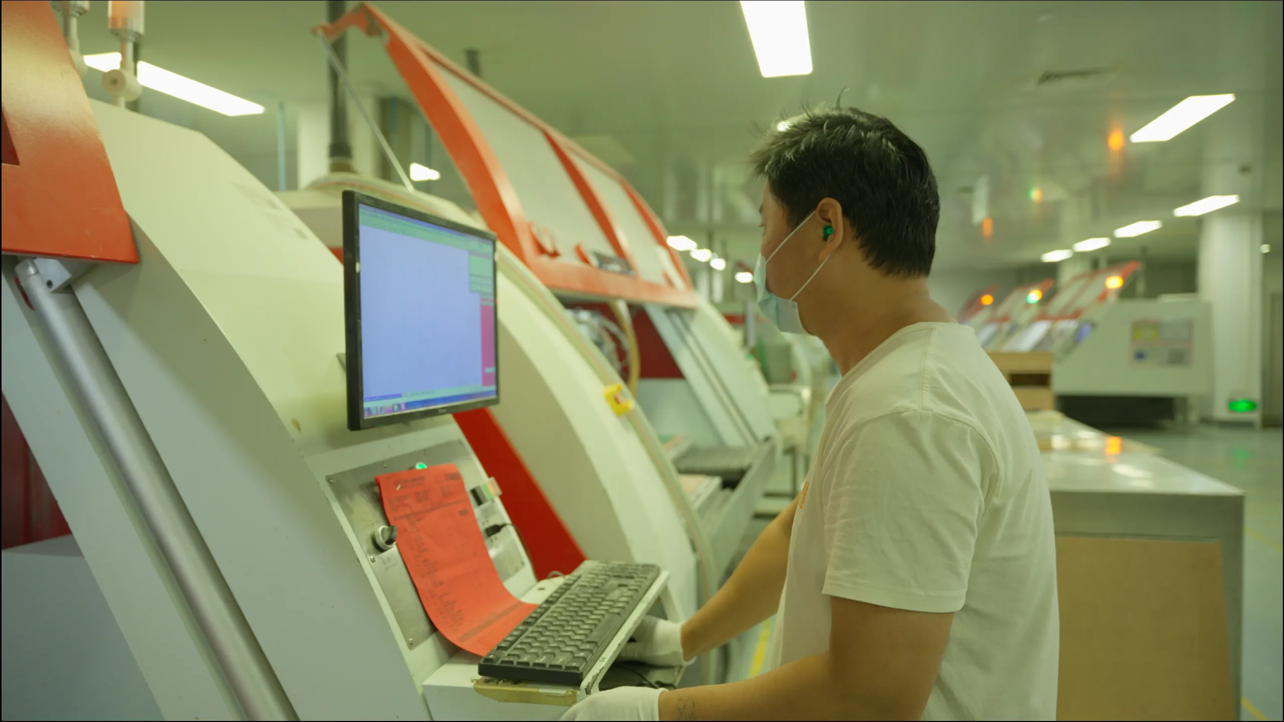
- Pre-Production Review: Before we start, ALLPCB engineers carefully check the design files. They look for difficult areas, like sharp corners, where burrs are likely to form. For these designs, they program a special 'deburring' process for the machine. This is an extra step where a tool goes back over the risky areas just to clean them up.
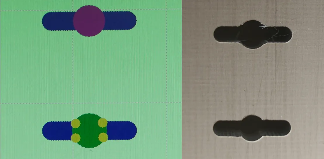
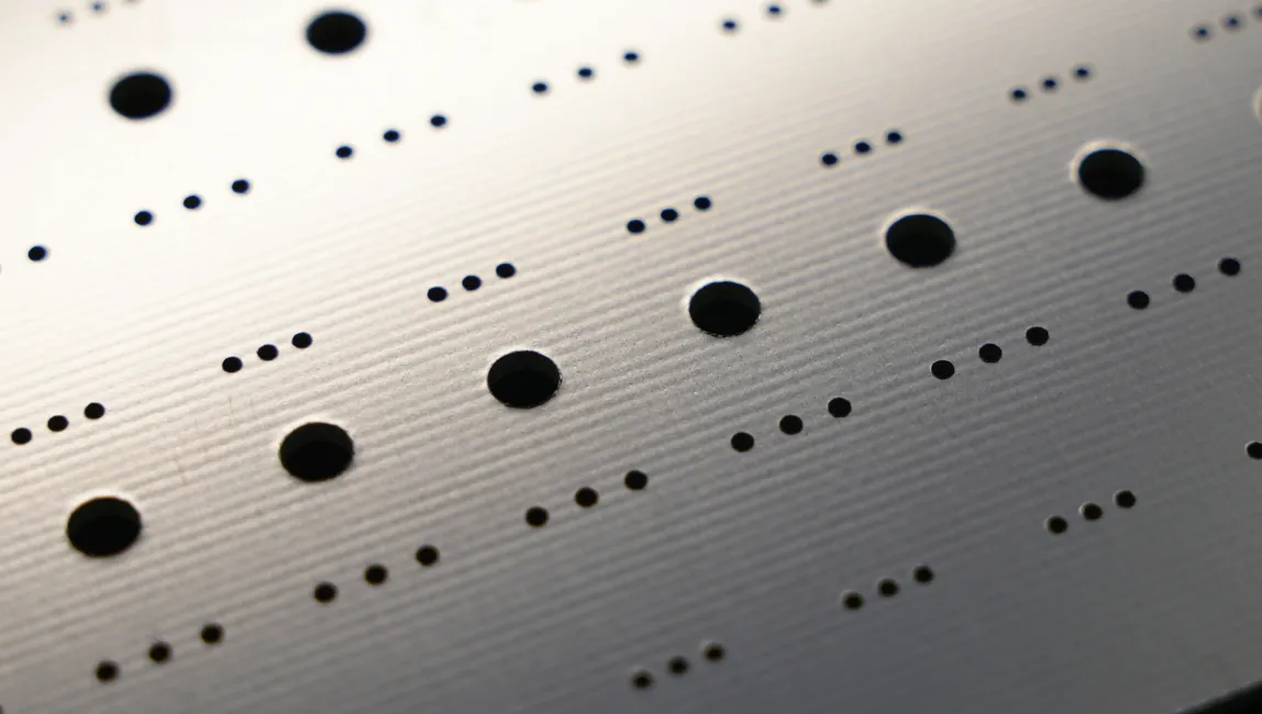
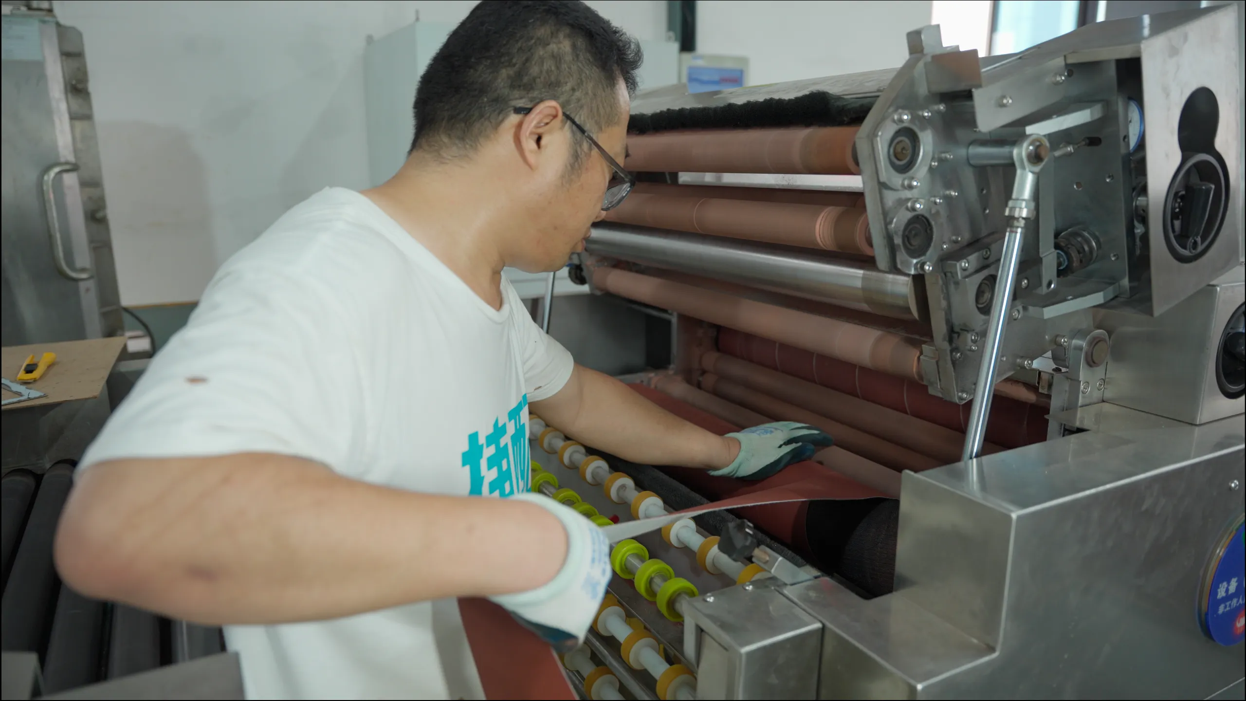
- Mandatory Post-Drilling Cleanup: After drilling, tiny ridges and burrs will always exist around the edge of the holes. These can block the copper plating process later. To solve this, every single board goes through a mandatory grinding process. A machine with special sandpaper smooths the board's surface and the edges of the holes. This is followed by a high-pressure water wash or ultrasonic cleaning to remove any leftover dust or debris.
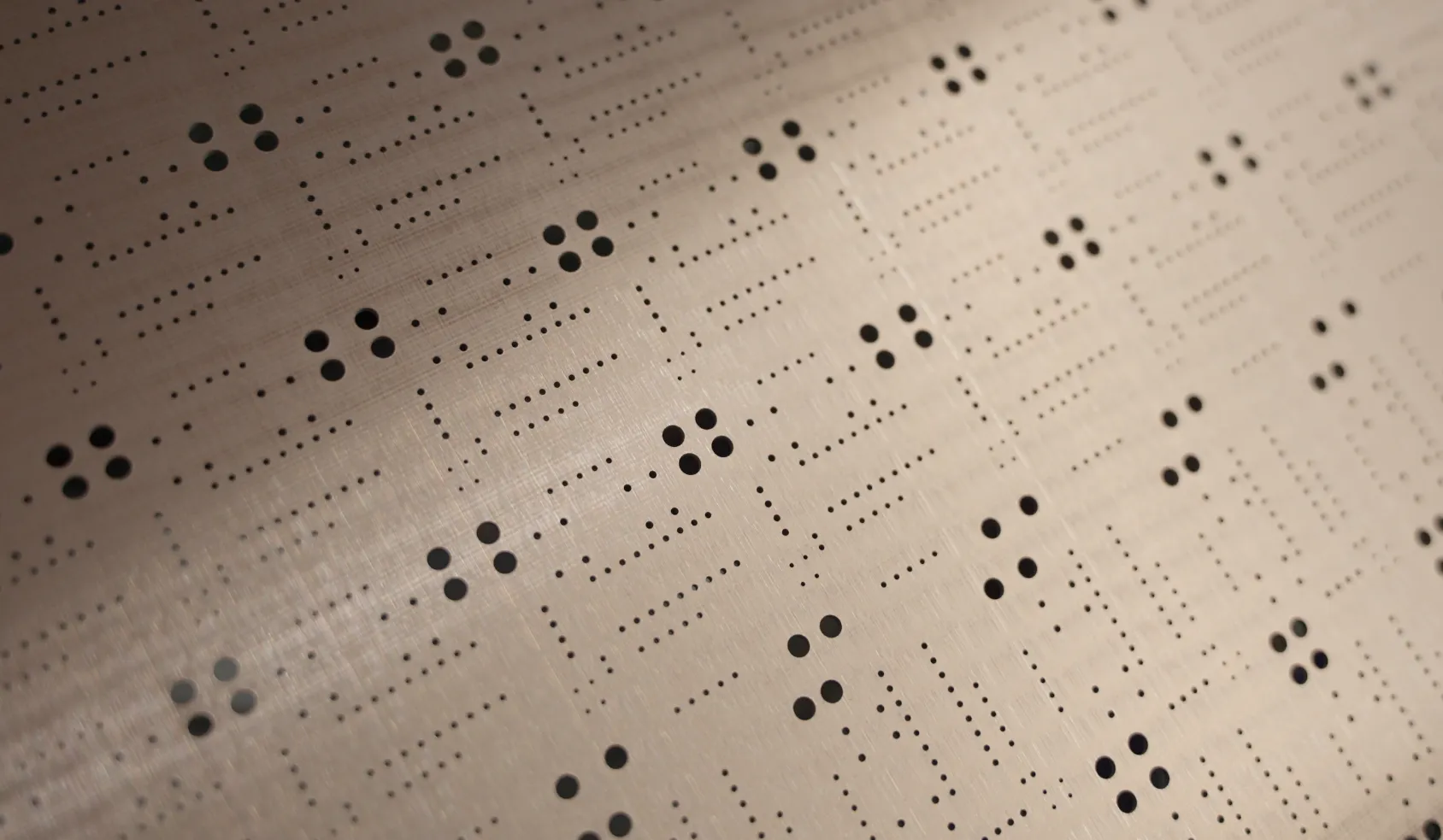
Board before clean-up
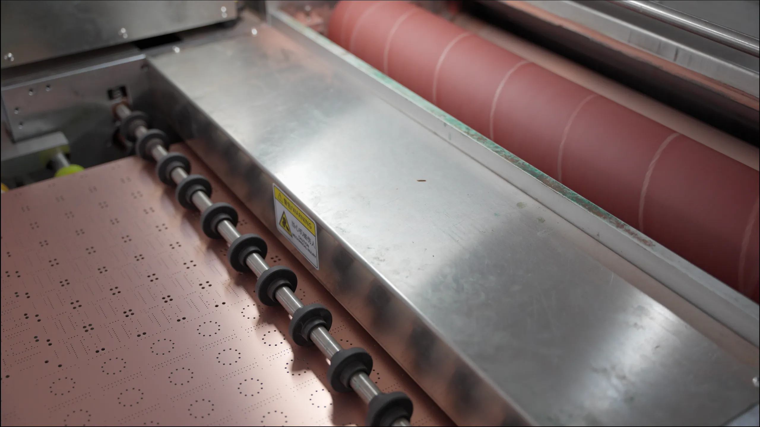
- Grinding Material Control: To make sure this grinding process is always effective, our production line workers replace the sandpaper on the machines after every 600 boards. This strict control guarantees a consistent and excellent smoothing effect on the surface of every board.
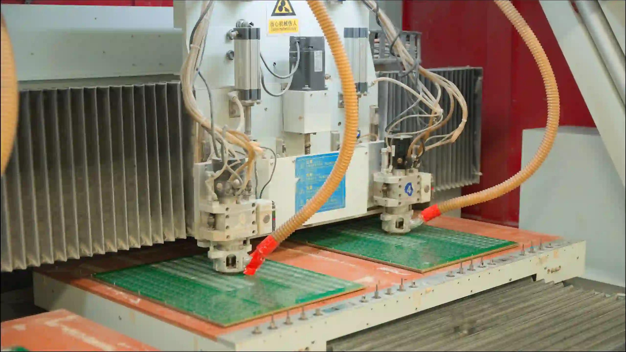
Stage 3: Final Shaping (Routing and V-Cutting)
Creating the final shape of the board is the last, critical step.
- Smart Routing: Our engineers adjust the machine settings (like tool speed and cutting path) for each specific board based on its material and thickness. Before the main production starts, every tool is checked and the program is tested.
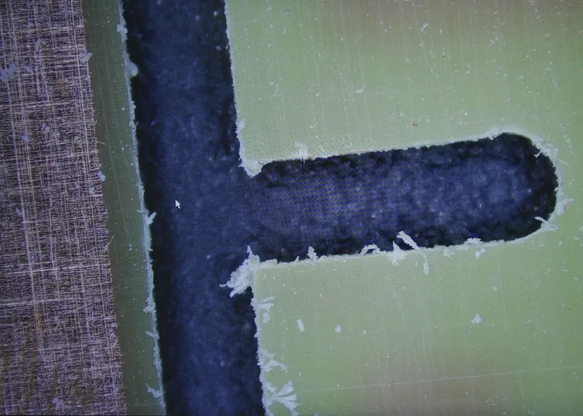
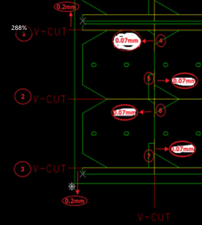
- Solving Difficult Designs: We specialize in handling complex board shapes. For example, a common problem is when a V-cut line meets a routed (cut-out) edge. This can create a large burr when the board is snapped. Our engineers solve this with a precise, multi-step process:
- First, they program the routing tool to cut the edge 0.2mm wider than the final design, staying clear of the V-cut area.
- Next, a separate, smaller milling tool is used to make a final, precise pass. It shaves off the last 0.07mm of material in the difficult area.
- Precise V-Cutting: For V-cuts, the depth of the cut is everything. We strictly control how much material is left to ensure the board snaps cleanly. Before we cut a large batch, we always produce a 'first article'—a single test board. We measure it carefully and do a trial snap to check that the edge is clean and smooth. Only after this test passes do we begin cutting the rest of the order.
Your Role in a Burr-Free PCB: Tips for Designers & Buyers
You can also help prevent burrs before your board ever reaches the factory.
For the PCB Designer:
- Round Sharp Inside Corners: Sharp 90-degree corners inside a cutout are hard for a routing tool to cut cleanly. If possible, add a small, rounded curve (a fillet) to these corners. This helps the tool move smoothly and creates a cleaner edge.
- Add Clear Notes: In your design files, include simple notes for the manufacturer, such as 'Deburr all holes and edges.' This tells the factory engineer that edge quality is important to you.
- Be Careful with Intersecting Lines: If your design has a V-cut line that crosses or touches a routed slot, make a note of it. This will alert the engineer to use special techniques to ensure a clean cut.
For the Person Ordering the PCBs:
- Choose the Right Panel Type: Boards can be separated from a panel using V-cuts or routing. V-cuts are cheaper but can leave a rougher edge. Routing leaves a very smooth edge but costs more. If edge quality is very important for your product, consider paying a little extra for a routed panel.
- Ask About Deburring: When you get a price quote, ask the manufacturer: 'Is deburring a standard part of your process?' This helps you understand exactly what you are paying for.
Working Together for Quality
A high-quality PCB is the result of teamwork between the designer and the manufacturer. By making smart choices in your design and communicating clearly with your supplier, you can greatly reduce the risk of burrs. When these good practices are combined with a manufacturer's detailed and controlled process, you can be confident that your circuit boards will be clean, reliable, and ready for your project.
At ALLPCB, we believe our job is to deliver more than just a circuit board; it's to deliver confidence. The pursuit of a burr-free PCB is a testament to our core philosophy: we don't aim for the lowest-cost processing, but for the kind of dependable quality that lets engineers rest easy. Every piece of customer feedback is a catalyst for improvement, pushing us to refine our processes even further.


