ALLPCB


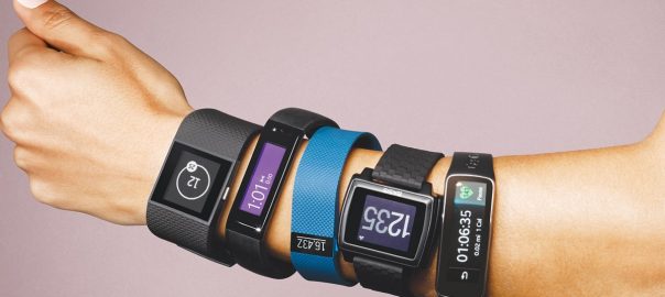
Wearable electronics are transforming industries like healthcare, fitness, and fashion, but prototyping these devices comes with unique hurdles. From flexible PCB assembly to small component soldering and wearable sensor integration, the assembly process can be complex. In this blog, we’ll explore the key challenges in wearable electronics assembly and provide practical solutions to help engineers and designers create successful prototypes. Whether you’re working on a fitness tracker or a medical monitoring device, this guide offers actionable insights to streamline your wearable prototype design process.
Introduction to Wearable Electronics Prototyping
Wearable electronics are devices designed to be worn on the body, such as smartwatches, health monitors, and augmented reality glasses. These gadgets need to be lightweight, comfortable, and durable while packing advanced technology into a small form factor. Prototyping wearable electronics involves creating functional models to test designs before mass production. However, the assembly process poses significant challenges due to the need for flexibility, precision, and integration of tiny components.
In this post, we’ll break down the major obstacles in wearable electronics assembly, including flexible PCB assembly, small component soldering, and wearable sensor integration. We’ll also share proven solutions to overcome these issues, ensuring your wearable prototype design meets performance and reliability standards.
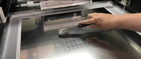
Challenge 1: Flexible PCB Assembly for Wearables
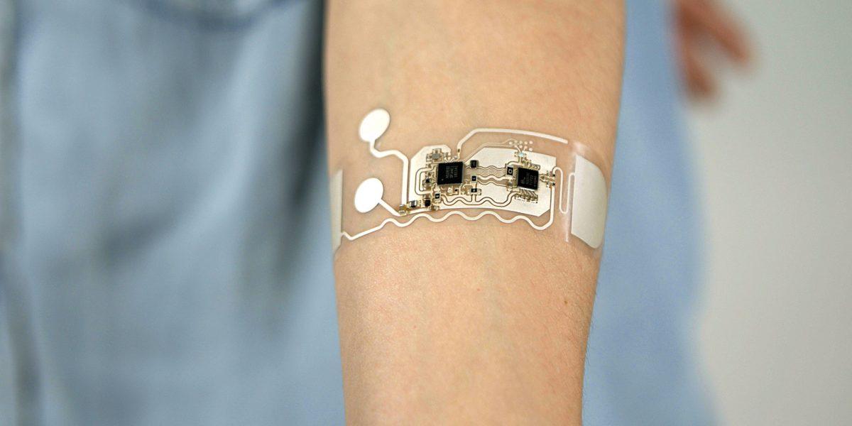
Flexible printed circuit boards (PCBs) are at the heart of most wearable electronics because they can bend and conform to the shape of the device or the human body. Unlike rigid PCBs, flexible PCBs are made from materials like polyimide, allowing them to fit into compact, curved spaces. However, assembling flexible PCBs for wearables presents several challenges.
Key Issues in Flexible PCB Assembly
- Material Fragility: Flexible substrates are thinner and more delicate than rigid boards, making them prone to tearing or damage during assembly. A typical flexible PCB might have a thickness of just 0.1mm to 0.2mm, requiring extreme care.
- Alignment Precision: Components must be placed with high accuracy on a flexible surface that may shift or deform during handling. Misalignment can lead to connection failures or short circuits.
- Thermal Stress: Soldering components on flexible PCBs can cause thermal stress, potentially warping the board or damaging the substrate. Standard soldering temperatures (around 260°C for lead-free solder) can be too high for some flexible materials.
Solutions for Flexible PCB Assembly
- Use Specialized Tools: Employ precision pick-and-place machines designed for flexible materials to ensure accurate component placement. These tools can handle delicate substrates without causing damage.
- Low-Temperature Soldering: Opt for low-temperature solder pastes (melting points around 138°C) to reduce thermal stress on the flexible PCB. This minimizes the risk of warping or material degradation.
- Reinforcement Layers: Add stiffeners or reinforcement layers to critical areas of the flexible PCB during assembly. This provides temporary rigidity for easier handling and component mounting without compromising overall flexibility.
By adopting these strategies, engineers can streamline flexible PCB assembly and create durable, reliable wearable prototypes that withstand bending and stretching during use.
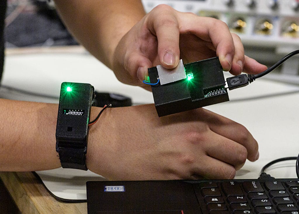
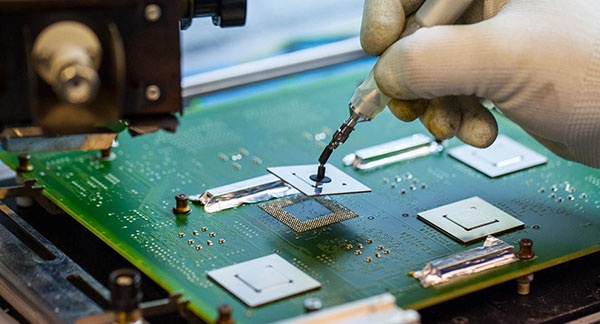
Challenge 2: Small Component Soldering in Wearable Devices
Wearable electronics often rely on micro-components, such as 0201 or 01005 size resistors and capacitors, to fit complex circuits into tiny spaces. Soldering these small components is a significant challenge during prototyping due to their size and the precision required.
Key Issues in Small Component Soldering
- Precision Placement: Components as small as 0.4mm x 0.2mm (01005 size) require exact placement. Even a slight deviation can cause poor connections or tombstoning, where one end of the component lifts off the pad.
- Solder Joint Reliability: Small solder joints are more susceptible to cracking under mechanical stress, especially in wearables that experience constant movement or vibration.
- Heat Management: Excessive heat during soldering can damage tiny components or nearby elements, leading to failures. For instance, overheating a micro-LED (common in wearables) can reduce its lifespan or alter its brightness output.
Solutions for Small Component Soldering
- Automated Soldering Equipment: Use automated reflow soldering systems with precise temperature control to ensure consistent heat distribution. These systems can maintain profiles within ±2°C of the target temperature, reducing the risk of overheating.
- Microscope-Assisted Assembly: For manual soldering during prototyping, use high-magnification microscopes (10x to 20x) to place and inspect tiny components accurately. This helps avoid misalignment and ensures strong solder joints.
- Advanced Solder Pastes: Select fine-particle solder pastes (Type 5 or Type 6) designed for micro-components. These pastes provide better control over solder volume, reducing defects like bridging or insufficient solder.
Mastering small component soldering is essential for creating compact, high-performance wearable electronics. With the right tools and materials, engineers can achieve reliable connections even in the smallest designs.
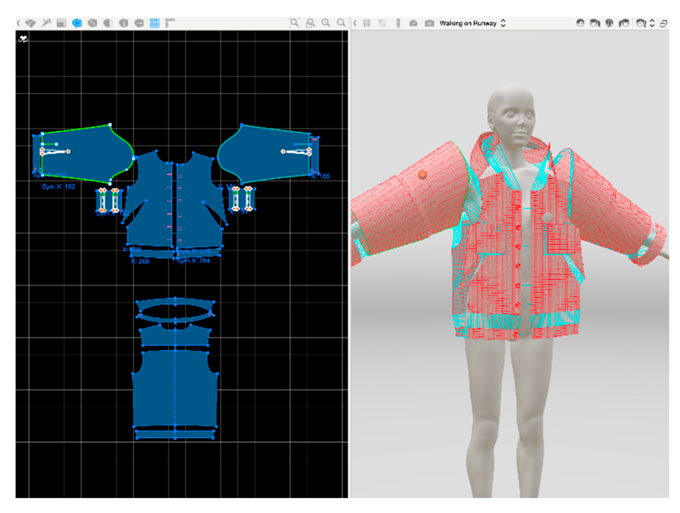
Challenge 3: Wearable Prototype Design and Ergonomics
Wearable prototype design goes beyond electronics—it must also prioritize user comfort and functionality. A wearable device that feels bulky or irritates the skin will fail to gain traction, no matter how advanced its features are.
Key Issues in Wearable Prototype Design
- Form Factor Constraints: The device must conform to the body’s shape, whether it’s a wristband, chest strap, or headgear. This limits the space available for components and batteries, often requiring custom PCB layouts.
- Weight Distribution: Uneven weight can make a wearable uncomfortable over long periods. For example, a smartwatch with a heavy battery on one side might cause wrist strain.
- Material Compatibility: Wearables are often in direct contact with skin, so materials must be hypoallergenic and sweat-resistant. Poor material choices can lead to skin irritation or corrosion of components.
Solutions for Wearable Prototype Design
- 3D Modeling and Simulation: Use 3D design software to simulate how the wearable fits on the body before building the prototype. This helps optimize the form factor and identify potential discomfort points early.
- Balanced Component Layout: Distribute weight evenly across the device by strategically placing heavier components like batteries. For instance, in a fitness band, position the battery and main chip on opposite sides for balance.
- Biocompatible Materials: Choose materials like medical-grade silicone or stainless steel for enclosures and straps. These materials are durable, skin-friendly, and resistant to moisture, ensuring long-term wearability.
A well-thought-out wearable prototype design not only enhances user experience but also reduces the need for costly redesigns later in the development process.
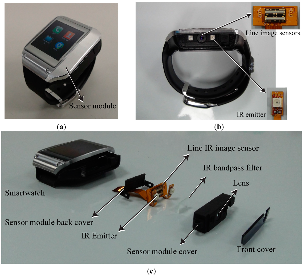
Challenge 4: Wearable Sensor Integration
Sensors are the core of many wearable electronics, enabling functions like heart rate monitoring, step counting, and temperature sensing. Integrating these sensors into a compact device while maintaining accuracy and reliability is a major challenge.
Key Issues in Wearable Sensor Integration
- Space Limitations: Sensors, along with their supporting circuitry, must fit into tight spaces without interfering with other components. A typical heart rate sensor module might require a footprint of 5mm x 5mm, which can be significant in a small device.
- Signal Interference: Wearables often operate in noisy environments, where electromagnetic interference (EMI) can disrupt sensor readings. For example, a poorly shielded accelerometer might pick up false motion data near other electronics.
- Power Consumption: Sensors need to operate continuously in many wearables, draining battery life. A poorly optimized sensor circuit might consume 1-2mA when idle, significantly reducing runtime.
Solutions for Wearable Sensor Integration
- Miniaturized Sensor Modules: Select ultra-compact sensor modules designed for wearables, which often combine multiple functions (e.g., heart rate and SpO2 sensing) into a single chip to save space.
- EMI Shielding: Incorporate shielding layers or ground planes around sensitive sensor circuits to minimize interference. For instance, placing a ground plane beneath a sensor can reduce EMI by up to 30% in some designs.
- Power Optimization: Use low-power sensors and implement sleep modes in firmware to reduce consumption during idle periods. Modern sensors can drop to microamp levels (e.g., 5μA) in sleep mode, extending battery life significantly.
Effective wearable sensor integration ensures accurate data collection without compromising the device’s size or power efficiency, making it a critical step in prototyping.
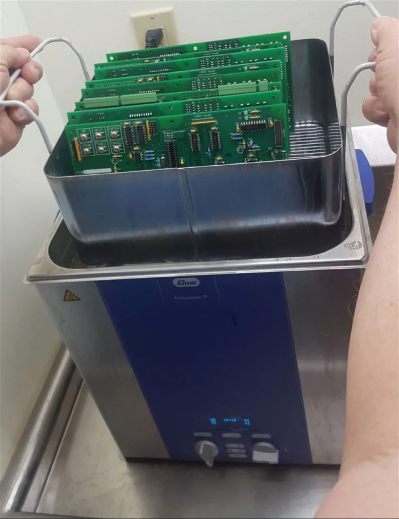
Overcoming General Assembly Challenges in Wearable Electronics
Beyond the specific challenges mentioned, wearable electronics assembly often faces broader issues like tight deadlines, cost constraints, and the need for iterative testing. Here are some overarching solutions to improve the prototyping process:
- Collaborate with Experts: Partner with experienced assembly teams who understand the nuances of wearable electronics. Their expertise can help avoid common pitfalls and speed up development.
- Rapid Prototyping Tools: Leverage quick-turn PCB fabrication and assembly services to produce multiple iterations of your design in a short time. This allows for faster testing and refinement.
- Thorough Testing Protocols: Test prototypes under real-world conditions, such as varying temperatures (e.g., -10°C to 50°C) and humidity levels (up to 85% RH), to ensure reliability before scaling to production.
By addressing both specific and general challenges, you can create wearable prototypes that are functional, user-friendly, and ready for market.
Conclusion: Building the Future of Wearable Electronics
Prototyping wearable electronics is a complex but rewarding process. Challenges like flexible PCB assembly, small component soldering, wearable prototype design, and wearable sensor integration can slow down development if not handled properly. However, with the right tools, techniques, and strategies, these obstacles become manageable. From using low-temperature soldering for delicate substrates to optimizing sensor power consumption, the solutions outlined in this guide can help engineers create cutting-edge wearables that meet user needs.
At ALLPCB, we’re committed to supporting innovators in bringing their wearable electronics to life. Our expertise in precision assembly and rapid prototyping ensures that your designs are built with the highest quality and efficiency. Start your next wearable project with confidence, knowing that every challenge has a solution waiting to be implemented.