 ALLPCB


Introduction
Flexible printed circuit boards, or flex PCBs, represent a pivotal advancement in electronics packaging, allowing circuits to bend, twist, and conform to irregular shapes without compromising functionality. For electrical engineers prototyping these boards, understanding design considerations and manufacturing techniques is essential to achieve reliable performance in compact applications. Prototyping flex PCBs enables early detection of mechanical and electrical issues, reducing costs and time in development cycles. This article examines flexible PCB design rules, flex PCB materials, bending radius flex PCB requirements, adhesive selection flex PCB options, and dynamic flex PCB applications. Factory-driven insights aligned with industry standards ensure prototypes transition smoothly to production. Engineers benefit from structured approaches that prioritize durability and manufacturability from the outset.
What Are Flexible PCBs and Why Prototype Them?
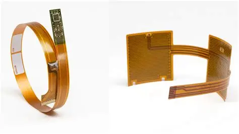
Flexible PCBs consist of thin, bendable substrates with embedded conductive traces, distinguishing them from rigid boards by their ability to accommodate movement and tight spaces. Common flex PCB materials include polyimide films for high-temperature resistance and polyester for cost-effective static uses, each influencing the board's flexibility and longevity. Prototyping is crucial because flex circuits undergo unique stresses during bending, which simulations alone cannot fully replicate. Real-world prototypes reveal issues like trace cracking or delamination early, informing design iterations. In dynamic flex PCB applications, such as sensors in robotics or displays in foldable devices, prototyping validates repeated flexing cycles. This step aligns with manufacturing realities, ensuring scalability and compliance with qualification criteria.
The relevance of prototyping intensifies in industries demanding miniaturization and reliability, where flex PCBs outperform rigid alternatives. Engineers prototype to test interconnections, material compatibility, and environmental resilience under actual conditions. Without this phase, production runs risk high failure rates due to overlooked mechanical vulnerabilities.
Key Flexible PCB Design Rules
Flexible PCB design rules govern trace routing, pad sizing, and bend areas to prevent failures from mechanical stress. Traces in bend zones require wider widths and curved paths rather than sharp angles to distribute strain evenly. Vias and pads must avoid flex regions or use staggered placements to minimize cracking risks. Coverlay openings demand precise alignment with underlying features for protection without restricting movement. Adhering to these rules during prototyping facilitates smoother manufacturing transitions.
Bending radius flex PCB specifications are central to design integrity. The minimum radius depends on layer count, copper thickness, and application type, with tighter radii possible in adhesiveless constructions. Engineers specify static bends conservatively to accommodate production tolerances. IPC-2223 provides sectional guidelines for flexible and rigid-flex designs, emphasizing bend zone isolation from rigid sections.
Layer stackups influence overall flexibility, with single-sided or double-sided flex favoring smaller radii than multilayers. Engineers balance electrical performance with mechanical limits by simulating strain distributions. Prototypes confirm these rules through bend testing, revealing any deviations from expected behavior.
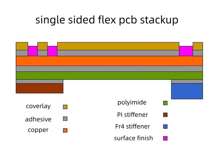
Flex PCB Materials and Adhesive Selection
Flex PCB materials form the foundation of performance, with substrates like polyimide offering superior thermal stability up to high processing temperatures and polyester suiting lower-cost, static applications. Copper foils, either rolled annealed for ductility or electrodeposited for finer lines, pair with these substrates. Coverlay films protect traces, mirroring solder mask functions but tailored for flex. Material selection during prototyping must consider compatibility with assembly processes and end-use environments.
Adhesive selection flex PCB construction critically affects bond strength and flex life. Acrylic adhesives provide good peel strength for static uses, while epoxy-based options excel in dynamic scenarios due to higher modulus. Adhesiveless laminates eliminate adhesive layers entirely, using direct copper bonding to polyimide for enhanced bend endurance. Factory insights recommend testing adhesion under humidity and temperature cycles to predict long-term reliability.
In multilayer flex, core and cover materials must match coefficients of thermal expansion to avoid warpage. Prototyping reveals interactions between materials and processes, such as lamination pressures influencing void formation. Engineers prioritize IPC-6013 qualification criteria for material performance verification.
Manufacturing Techniques for Flexible PCB Prototypes
Prototyping flexible PCBs employs scaled-down versions of production processes, starting with panelization of multiple designs on carrier sheets for efficiency. Photolithographic patterning defines traces on copper-clad laminates, followed by etching and coverlay application. Laser drilling or photo-defined vias enable interconnections in dense areas. Lamination bonds layers under controlled heat and pressure, critical for void-free interfaces.
For prototypes, manufacturers often use adhesive-based builds for versatility, transitioning to adhesiveless for high-volume dynamic flex PCB applications. Stiffeners attach to rigid zones post-flex fabrication, enhancing component mounting stability. Electrical testing, including continuity and insulation resistance, precedes mechanical bend evaluations. These techniques ensure prototypes mirror production quality.
IPC-6013 outlines performance specifications for flexible boards, guiding acceptance criteria like plating thickness and flex endurance. Prototyping lots undergo accelerated life testing to simulate field conditions. Engineers collaborate with fabricators to refine panel layouts, minimizing material waste.
Best Practices for Dynamic Flex PCB Applications
Dynamic flex PCB applications, including hinges in consumer electronics and actuators in medical devices, demand robust designs against millions of cycles. Best practices include isolating traces from extreme bend axes and using hatched copper planes to reduce stress concentrations. Component placement favors rigid-flex hybrids, with flex tails handling motion. Prototyping incorporates cyclic bend fixtures to quantify fatigue life.
Common pitfalls involve undersizing bend radii or neglecting coverlay shrinkage, leading to trace fractures. Engineers mitigate these by incorporating strain-relief features like teardrop pads and gradual tapers. Material upgrades to polyimide with rolled copper enhance cycle counts. Factory-driven validation confirms compliance before scaling.
Adhesive selection flex PCB choices prioritize low-outgassing types for vacuum environments. Multilayer dynamics require symmetric stackups to prevent curl. Prototypes inform iterative refinements, ensuring reliability in applications like wearable health monitors.
Conclusion
Prototyping flexible PCBs bridges innovative designs with manufacturable realities, emphasizing flexible PCB design rules, appropriate flex PCB materials, precise bending radius flex PCB management, strategic adhesive selection flex PCB builds, and tailored dynamic flex PCB applications. Electrical engineers leveraging these considerations achieve prototypes that withstand real-world demands. Alignment with standards like IPC-2223 and IPC-6013 fortifies outcomes. Future advancements in materials will further expand flex capabilities, but foundational practices remain key. Prioritizing structured prototyping yields reliable, high-performance circuits.
FAQs
Q1: What are the primary flexible PCB design rules for bend areas?
A1: Flexible PCB design rules prioritize curved trace routing, wider conductors in flex zones, and avoidance of vias in high-strain regions to distribute mechanical stress. Bend radii scale with thickness, typically larger for dynamic uses. Prototyping validates these rules through fatigue testing, ensuring compliance with sectional standards. This approach prevents cracking and extends service life in compact assemblies.
Q2: How do flex PCB materials impact prototyping outcomes?
A2: Flex PCB materials like polyimide provide thermal resilience, while polyester suits budget static prototypes. Copper type influences ductility, with rolled annealed favoring bends. During prototyping, material interactions with processes like lamination reveal compatibility issues early. Selecting based on application needs optimizes flex life and manufacturability.
Q3: What factors determine bending radius flex PCB specifications?
A3: Bending radius flex PCB depends on layer count, copper weight, and static versus dynamic use, with dynamic requiring larger multiples of thickness for endurance. Design guidelines recommend conservative values accounting for tolerances. Prototypes confirm radii via bend testing, adjusting for production variations. Proper specification avoids trace fatigue in applications like foldables.
Q4: Why is adhesive selection flex PCB critical in dynamic applications?
A4: Adhesive selection flex PCB affects peel strength and flex cycles, with epoxy outperforming acrylic in repeated bending. Adhesiveless constructions enhance reliability by eliminating weak interfaces. Prototyping tests adhesion under cycles and environments, informing choices. This ensures integrity in dynamic flex PCB applications such as robotics.


