If you're looking for effective PCB routing guidelines, you're in the right place. A well-designed PCB layout is crucial for ensuring your electronic project works reliably and efficiently. Poor routing can lead to signal interference, power issues, or even complete board failure. In this comprehensive guide, we'll explore key PCB layout considerations and best practices, with a focus on routing techniques to help you achieve optimal performance. From component placement to trace management, we've got you covered with actionable tips and detailed insights.
Why PCB Layout Matters
The layout of a printed circuit board (PCB) is more than just arranging components and drawing traces. It directly impacts the board's functionality, signal integrity, and manufacturability. A thoughtful design can reduce noise, improve thermal management, and ensure your board performs as intended. On the other hand, neglecting layout considerations can result in costly redesigns or unreliable products. Whether you're a beginner or an experienced engineer, understanding these principles is essential for creating high-quality boards.
Key Considerations for PCB Layout Design
Before diving into routing guidelines, let's cover the foundational aspects of PCB layout. These considerations set the stage for effective routing and overall board performance.
1. Component Placement
Component placement is the first step in PCB layout and significantly affects routing efficiency. Place components logically based on their function and connectivity. For example, keep high-speed components close to each other to minimize trace lengths and reduce signal delay. Group related components, such as power supply circuits, near their respective connectors to simplify power distribution.
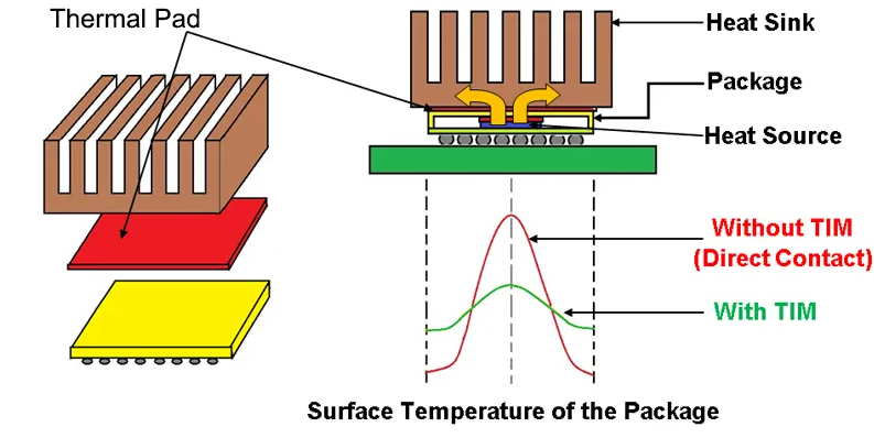
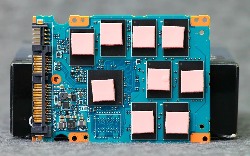
Additionally, consider thermal management during placement. High-power components like voltage regulators or microcontrollers generate heat and should be placed away from heat-sensitive parts. Allow space for heat sinks or ventilation if needed. As a rule of thumb, aim for at least 0.5 inches of clearance around high-heat components to prevent thermal interference.
2. Power and Ground Planes
A solid power and ground plane setup is critical for reducing noise and ensuring stable voltage distribution. Dedicate entire layers to power and ground in multilayer boards to provide a low-impedance path for current. This approach minimizes voltage drops and electromagnetic interference (EMI). For instance, in a 4-layer board, assign the second layer to ground and the third to power for optimal performance.
Make sure to place decoupling capacitors close to the power pins of integrated circuits (ICs). A typical value for these capacitors is 0.1 μF, which helps filter out high-frequency noise. Connect these capacitors directly to the ground plane with short traces or vias to maximize their effectiveness.
3. Signal Integrity
Signal integrity is a major concern, especially in high-speed designs. Long traces or improper routing can cause signal reflections, crosstalk, or delays. To maintain signal integrity, keep critical signal traces short and direct. For high-speed signals like USB or HDMI, aim for trace lengths under 6 inches to avoid significant delays (assuming a signal speed of approximately 6 inches per nanosecond in FR-4 material).
Also, avoid routing high-speed signals near noisy components like switching regulators. Use differential pair routing for signals like USB or Ethernet, maintaining consistent spacing (typically 5-10 mils) between the pair to prevent imbalance.
Effective PCB Routing Guidelines
Now that we've covered the basics, let's focus on routing—the heart of PCB layout. Proper routing ensures signals travel efficiently without interference. Here are some best practices to follow for effective PCB routing.
1. Keep Traces Short and Direct
One of the golden rules of PCB routing is to keep traces as short and direct as possible. Longer traces increase resistance and inductance, which can degrade signal quality and introduce noise. For example, in a digital circuit with a clock signal running at 50 MHz, a trace longer than 3 inches may cause timing issues due to propagation delay.
When routing, prioritize critical nets like clock signals or high-speed data lines first. Use 45-degree angles instead of sharp 90-degree turns to reduce signal reflections. Sharp corners can act as antennas, radiating EMI and disrupting performance.
2. Optimize Trace Width and Spacing
Trace width and spacing are crucial for managing current capacity and preventing crosstalk. For power traces, use wider traces to handle higher currents without overheating. A common guideline is to use a trace width of 10 mils per ampere of current. So, for a 2A power line, a 20-mil trace width is a good starting point.
For signal traces, maintain adequate spacing to avoid crosstalk. A general rule is to keep spacing at least three times the trace width (3W rule) for adjacent signals. For example, if your trace width is 6 mils, ensure at least 18 mils of separation from the next trace to minimize interference.
3. Use Differential Pair Routing for High-Speed Signals
In high-speed designs, differential pairs are often used to transmit data with minimal noise. These pairs consist of two traces carrying complementary signals, such as in USB or LVDS interfaces. To route differential pairs effectively, keep the traces parallel and maintain equal length. A length mismatch of even 10 mils can introduce skew, disrupting signal timing.
Additionally, ensure the spacing between the two traces in the pair is consistent. A typical spacing for differential pairs is 5-8 mils, depending on the impedance requirements (often 90-100 ohms for USB). Use simulation tools if possible to verify impedance matching during the design phase.
4. Avoid Crossing Traces on the Same Layer
Crossing traces on the same layer can create unintended coupling or noise. If traces must cross, use a different layer by adding vias. However, minimize the use of vias in high-speed signals, as they can introduce inductance and affect signal integrity. When using vias, place them strategically and ensure they connect to a ground plane to reduce EMI.
For multilayer boards, dedicate specific layers to horizontal and vertical routing. For instance, in a 4-layer board, route horizontal traces on the top layer and vertical traces on the bottom layer to avoid unnecessary crossings.
5. Route Power and Ground Traces First
Always prioritize routing power and ground traces before signal traces. This ensures a stable reference for all signals and reduces the risk of noise. Connect power traces directly to the power plane with wide paths to handle current demands. Similarly, ground traces should connect to the ground plane with multiple vias for a low-impedance return path.
For analog and digital circuits on the same board, separate their ground planes to prevent noise from digital signals interfering with sensitive analog components. Connect the two ground planes at a single point near the power supply to avoid ground loops.
Thermal Management in PCB Layout
Thermal management is often overlooked but is vital for PCB reliability. Excessive heat can damage components or degrade performance over time. Here are some tips to manage heat effectively during layout design.
1. Use Thermal Vias
Thermal vias are small holes filled with conductive material that transfer heat from hot components to a heat-dissipating layer, such as a ground plane. Place thermal vias under high-power components like power transistors or LEDs. A typical arrangement is a grid of 4-6 vias with a diameter of 10-12 mils each, spaced about 50 mils apart, to maximize heat dissipation.
2. Add Copper Pours for Heat Spreading
Copper pours or planes act as heat spreaders, distributing thermal energy across the board. Connect high-heat components to large copper areas on the PCB surface. Ensure these areas are linked to thermal vias or heat sinks for better heat transfer. For example, a 1-square-inch copper pour can reduce the temperature of a power IC by up to 10°C under typical operating conditions.
Design for Manufacturability (DFM)
A great PCB layout isn't just about performance—it must also be easy to manufacture. Ignoring manufacturability can lead to production delays or increased costs. Keep these points in mind during the design process.
1. Follow Minimum Trace and Space Rules
Every PCB manufacturer has specific capabilities for minimum trace width and spacing. Standard values are often 6 mils for trace width and 6 mils for spacing, but check with your fabrication house to confirm. Designing below these limits can result in manufacturing errors or higher costs due to specialized processes.
2. Place Fiducials for Assembly
Fiducials are reference marks on the PCB that help automated assembly machines align components accurately. Place at least three fiducials on the board, typically near the corners, with a diameter of 40 mils and a clearance of 80 mils around each. This ensures precise placement during assembly, reducing errors.
Common Mistakes to Avoid in PCB Layout
Even experienced designers can make mistakes during PCB layout. Here are some common pitfalls to watch out for:
- Overcrowding Components: Placing components too close together can make routing difficult and increase heat buildup. Leave at least 10-15 mils of clearance between components for easier assembly and heat dissipation.
- Ignoring Impedance Matching: For high-speed designs, failing to match impedance can lead to signal reflections. Use controlled impedance traces (e.g., 50 ohms for RF signals) and verify with simulation tools.
- Poor Via Placement: Placing vias in high-current paths or near sensitive signals can introduce noise or inductance. Always connect vias to ground planes for shielding.
Tools and Resources for PCB Layout
Modern PCB design software offers powerful features to simplify layout and routing. These tools often include simulation capabilities to test signal integrity and thermal performance before fabrication. Look for software with built-in design rule checks (DRC) to catch errors like insufficient trace spacing or unconnected nets. Many tools also provide libraries of pre-designed components to speed up the process.
Additionally, online resources such as application notes, forums, and tutorials can offer valuable insights into specific layout challenges. Staying updated on industry standards, like IPC guidelines, ensures your designs meet professional requirements.
Conclusion
Creating an effective PCB layout requires careful planning, attention to detail, and adherence to best practices. By focusing on component placement, signal integrity, and thermal management, you can design boards that perform reliably under various conditions. Effective PCB routing guidelines, such as keeping traces short, optimizing widths, and using differential pairs, are essential for minimizing noise and ensuring signal quality. Moreover, designing with manufacturability in mind saves time and reduces costs during production.
Whether you're working on a simple hobby project or a complex industrial application, these PCB layout considerations and best practices will guide you toward success. Take the time to plan your design, use the right tools, and double-check your work. A well-designed PCB not only functions better but also stands the test of time in real-world applications.
 ALLPCB


