ALLPCB


If you're looking to enhance your printed circuit board (PCB) performance, one often overlooked factor is solder mask thickness. The right solder mask thickness can improve insulation, durability, planarity, and even impedance control, while preventing issues like warpage. In this comprehensive guide, we'll dive deep into how optimizing solder mask thickness can elevate your PCB designs and provide actionable tips to achieve the best results.
What Is Solder Mask and Why Does Thickness Matter?
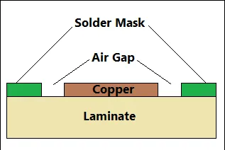
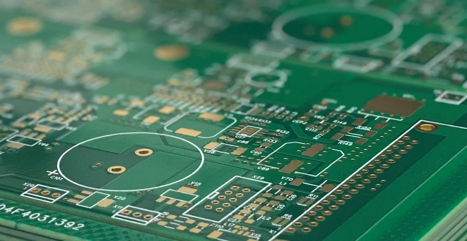
Solder mask is a thin protective layer applied to the copper traces of a PCB. It serves multiple purposes: it prevents solder from bridging between components, insulates the traces to avoid short circuits, and protects the board from environmental factors like moisture and dust. But why does the thickness of this layer matter?
The thickness of the solder mask directly impacts several critical aspects of PCB performance, including solder mask insulation, solder mask durability, and solder mask impedance control. A layer that's too thin may fail to provide adequate protection, while one that's too thick can cause uneven surfaces or affect signal integrity. Striking the right balance is key to ensuring your PCB functions reliably under various conditions.
The Role of Solder Mask Thickness in PCB Performance
Let’s break down how solder mask thickness influences different aspects of PCB performance. Understanding these factors will help you make informed decisions during the design and manufacturing process.
1. Solder Mask Insulation: Protecting Against Short Circuits
Solder mask insulation is one of the primary functions of this layer. The solder mask acts as a barrier between conductive traces, preventing unintended electrical connections. If the solder mask is too thin, typically less than 0.8 mils (20 micrometers), it may not provide sufficient dielectric strength, leading to potential breakdowns under high-voltage conditions.
For high-voltage applications, a thicker solder mask—around 1.2 to 1.5 mils (30-38 micrometers)—is often recommended to ensure proper insulation. However, the exact thickness depends on the operating environment and voltage levels of your design. Always refer to industry standards like IPC-SM-840 for guidance on insulation requirements.
2. Solder Mask Durability: Enhancing Longevity
Solder mask durability is crucial for protecting the PCB from physical and environmental damage. A thicker solder mask can better resist scratches, abrasion, and chemical exposure during assembly and operation. For example, in harsh environments where PCBs are exposed to moisture or corrosive substances, a thickness of 1.0 to 1.5 mils (25-38 micrometers) can significantly extend the board’s lifespan.
On the other hand, an overly thick solder mask may crack under thermal stress, especially during reflow soldering processes where temperatures can exceed 260°C. Balancing thickness with flexibility is essential to maintain durability without compromising the board’s integrity.
3. Solder Mask Planarity: Ensuring a Flat Surface
Solder mask planarity refers to the flatness of the solder mask layer across the PCB surface. Uneven solder mask thickness can lead to height variations, which may cause issues during component placement or soldering. For instance, if the solder mask is thicker in some areas (above 2.0 mils or 50 micrometers), it can create bumps that interfere with surface-mount components, leading to poor solder joints.
To achieve optimal planarity, aim for a uniform solder mask thickness of 0.8 to 1.2 mils (20-30 micrometers). This range ensures a smooth surface while providing adequate protection. Advanced manufacturing techniques, such as precise screen printing or photoimageable solder masks, can help maintain consistent thickness across the board.
4. Solder Mask Impedance Control: Impact on Signal Integrity
Solder mask impedance control is a critical consideration for high-frequency PCB designs. The solder mask acts as a dielectric layer, and its thickness influences the characteristic impedance of the traces. A thicker solder mask can lower the impedance, which might affect signal integrity in high-speed circuits operating at frequencies above 1 GHz.
For controlled impedance designs, the solder mask thickness typically needs to be tightly controlled within ±0.2 mils (±5 micrometers) of the target value, often around 0.8 mils (20 micrometers). This precision ensures that signal speeds—often in the range of 3 to 5 picoseconds per inch for high-speed signals—remain consistent. Working closely with your manufacturing partner to define and verify these parameters is essential for applications like RF or high-speed digital circuits.
5. Solder Mask Warpage: Preventing Board Deformation
Solder mask warpage occurs when uneven thickness or improper curing of the solder mask causes the PCB to bend or deform. Warpage is especially problematic for large or thin boards, as it can lead to assembly issues or mechanical stress on components. A solder mask that’s too thick, exceeding 2.0 mils (50 micrometers), or unevenly applied can create internal stresses during thermal cycling, worsening warpage.
To minimize warpage, maintain a uniform solder mask thickness of 0.8 to 1.2 mils (20-30 micrometers) and ensure proper curing processes. Following industry guidelines, such as those from IPC-6012, can help control warpage and keep the board within acceptable flatness tolerances, typically less than 0.75% of the board’s diagonal dimension.
Industry Standards for Solder Mask Thickness
Adhering to solder mask standards is vital for ensuring reliability and consistency in PCB manufacturing. The most widely recognized standard is IPC-SM-840, which outlines the performance requirements for solder mask materials and application. According to this standard, the typical solder mask thickness should range from 0.8 to 1.5 mils (20-38 micrometers) for most applications, depending on the PCB class and intended use.
For specific applications, such as high-reliability aerospace or medical devices, stricter tolerances may apply. IPC-6012 and IPC-A-600 provide additional guidelines for acceptable thickness variations and visual inspection criteria. Always consult these standards during the design phase to ensure compliance and avoid costly rework.
How to Optimize Solder Mask Thickness for Your PCB
Now that we’ve covered the impact of solder mask thickness on various performance aspects, let’s explore practical steps to optimize it for your specific needs.
Step 1: Define Your PCB Requirements
Start by identifying the operating conditions of your PCB. Will it be used in a high-voltage environment requiring robust solder mask insulation? Does it need to handle high-frequency signals where solder mask impedance control is critical? Understanding these requirements will help you determine the ideal thickness range.
Step 2: Select the Right Solder Mask Material
Different solder mask materials have varying properties that affect thickness and performance. Liquid photoimageable (LPI) solder masks, for instance, allow for precise control over thickness and are ideal for high-density designs. Epoxy-based masks, on the other hand, offer greater solder mask durability for rugged applications but may be harder to apply uniformly.
Step 3: Collaborate with Your Manufacturer
Work closely with your PCB manufacturer to ensure the solder mask is applied within the desired thickness range. Provide detailed specifications in your design files, including target thickness and tolerance levels. Request test coupons or cross-sectional analysis to verify the applied thickness meets your expectations.
Step 4: Test and Validate
After manufacturing, test your PCBs under real-world conditions to confirm that the solder mask performs as expected. Check for issues like warpage, insulation failures, or signal integrity problems. If necessary, adjust the thickness or application method for future batches to optimize performance.
Common Challenges and Solutions with Solder Mask Thickness
Even with careful planning, issues related to solder mask thickness can arise. Here are some common challenges and how to address them:
- Uneven Thickness Leading to Poor Planarity: Use advanced application methods like LPI solder masks and ensure proper curing to achieve uniform solder mask planarity.
- Cracking Due to Thermal Stress: Avoid excessively thick layers and select materials with good thermal resistance to enhance solder mask durability.
- Impedance Variations in High-Speed Designs: Tighten thickness tolerances and perform impedance testing to maintain solder mask impedance control.
- Warpage in Large Boards: Balance thickness across the board and follow proper curing processes to prevent solder mask warpage.
Conclusion: Achieving Peak PCB Performance with Optimal Solder Mask Thickness
Optimizing solder mask thickness is a powerful way to improve your PCB’s overall performance. By carefully considering factors like solder mask insulation, solder mask durability, solder mask planarity, solder mask impedance control, and solder mask warpage, you can design boards that meet the highest standards of reliability and functionality.
Start by defining your specific requirements, selecting the right materials, and adhering to solder mask standards like IPC-SM-840. Collaborate with your manufacturing partner to ensure precision in application and validate the results through thorough testing. With the right approach, a well-optimized solder mask thickness can be the difference between a good PCB and a great one.
By following the guidelines and insights shared in this post, you’re well on your way to creating high-performing PCBs tailored to your unique needs. Keep experimenting and refining your designs to stay ahead in the ever-evolving world of electronics.