ALLPCB


Overview
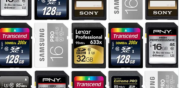
NAND Flash is widely used across consumer devices such as SD cards, smartphones and tablets, as well as in data center and enterprise applications, due to its high performance, large capacity, low power consumption and low cost. This article explains the ONFI (Open NAND Flash Interface) standard that defines the interface between NAND Flash devices and controllers.
Definition
ONFI (Open NAND Flash Interface) is a protocol that specifies the communication interface between NAND Flash memory and controllers. It defines command sequences and data transfer formats so controllers can perform read, program and erase operations reliably.
ONFI is developed and maintained by an industry working group of more than 100 companies that manufacture, design or use NAND Flash devices, including major members such as Intel and Micron. The working group publishes component-level interface specifications, connector and module form-factor definitions to simplify NAND integration into consumer electronics, computing platforms and other applications requiring large-capacity solid-state storage.
Specifications
The ONFI specification covers key areas including:
- Electrical interface: voltage levels, signal timing and protocol between the NAND device and the controller.
- Command set: commands and command sequences used by the controller to access and control the NAND device, including read, program and erase operations.
- Data transfer modes: supported transfer modes such as asynchronous and synchronous transfers, multi-plane operations and multi-channel access.
- Timing parameters: timing characteristics including setup and hold times, maximum clock frequency and other timing constraints needed for reliable data transfer.
Trends
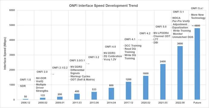
By providing an open interface standard, ONFI has improved compatibility and interoperability among NAND devices from different vendors, expanded the supply base for standardized devices and reduced product development time. Since the first ONFI release in December 2006, the interface data rate has evolved from an initial 50 Mbps to the current 3600 Mbps. The following figure shows the evolution trend of ONFI interface speeds.
Technical Challenges and Developments
ONFI has evolved to ONFI 5.x. ONFI 5.x introduced NV-LPDDR4 technology, increasing the interface rate from ONFI 5.0’s 2400 Mbps to ONFI 5.1’s 3600 Mbps. To address signal integrity challenges at these higher speeds, in addition to enhanced write calibration and VrefQ calibration, ONFI 5.x introduces asymmetric DQS design and adaptive equalizer techniques. Decision Feedback Equalizer (DFE) uses weighted feedback from previous channel outputs to the input decision, helping to mitigate post-cursor inter-symbol interference. Although NV-DDR3 and NV-LPDDR4 can support the same maximum interface rate, NV-LPDDR4 with LTT technology can significantly reduce read power.
From ONFI 1.0 to ONFI 5.1 the interface rate has increased rapidly, but the formats for command, address and data transfers have remained largely unchanged. While bus rates have increased and reduced data transfer latency, command and address transfer latencies have not improved, which reduces overall bus utilization.
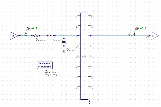
Simulation
On SIDesigner simulation platforms, configuring IBIS models for the controller and the NAND device and providing the intermediate S-parameters enables simulation of NAND Flash using the ONFI protocol.