 ALLPCB


In the world of PCB design, achieving optimal power integrity is crucial for ensuring the performance and reliability of electronic devices. A key factor in this process is mastering PDN impedance—Power Distribution Network impedance. Whether you're targeting a specific PDN impedance target, conducting PDN impedance measurement, designing a low impedance PDN, running PDN impedance simulation, or focusing on PDN impedance optimization, understanding this concept is vital for success. In this guide, we’ll break down everything you need to know about PDN impedance and provide actionable insights to enhance your power integrity design.
This comprehensive blog will walk you through the fundamentals of PDN impedance, why it matters, and how to manage it effectively in your PCB projects. From setting targets to simulation and optimization, we’ve got you covered with practical tips and detailed explanations.
What is PDN Impedance and Why Does It Matter?
PDN impedance refers to the opposition to the flow of alternating current (AC) within the Power Distribution Network of a printed circuit board (PCB). The PDN is responsible for delivering stable power to all components on the board, and its impedance directly impacts how well it can handle transient currents and maintain voltage stability. High impedance can lead to voltage drops, noise, and signal integrity issues, while a low impedance PDN ensures cleaner power delivery and better performance.
Power integrity design hinges on controlling PDN impedance to prevent issues like electromagnetic interference (EMI) and power rail noise. As modern devices operate at higher speeds and lower voltages (often below 1V for advanced ICs), even small fluctuations—such as a 50mV ripple—can cause significant problems. This makes mastering PDN impedance a top priority for engineers working on high-speed or high-performance electronics.
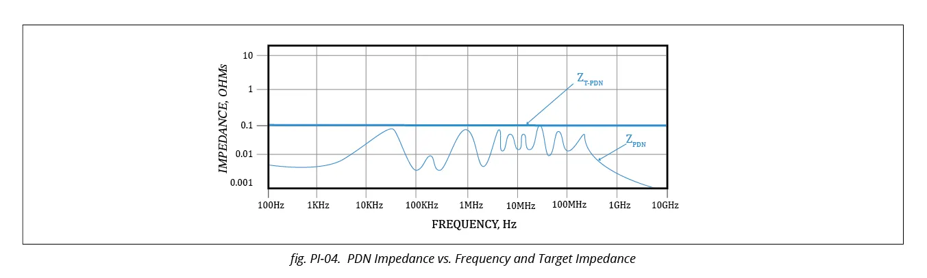
Setting a PDN Impedance Target for Optimal Performance
One of the first steps in power integrity design is defining a PDN impedance target. This target represents the maximum allowable impedance that ensures voltage noise remains within acceptable limits, even during worst-case transient current demands. For example, if a processor draws a sudden 10A current spike, the PDN must maintain voltage stability within a tolerance of ±5% (e.g., 50mV for a 1V rail). To calculate the target impedance, use the formula:
Z_target = ΔV / I_transient
Here, ΔV is the allowable voltage ripple, and I_transient is the maximum transient current. For a 1V rail with a 50mV ripple and 10A transient current, the target impedance would be 5mΩ (0.05V / 10A). Achieving this low impedance across a wide frequency range (from DC to several GHz) is a challenge, but it’s critical for modern designs.
Setting a realistic PDN impedance target depends on the specific requirements of your components, such as the power supply type and the sensitivity of ICs to noise. Start by consulting datasheets for allowable noise margins and current profiles, then use these values to define your target.
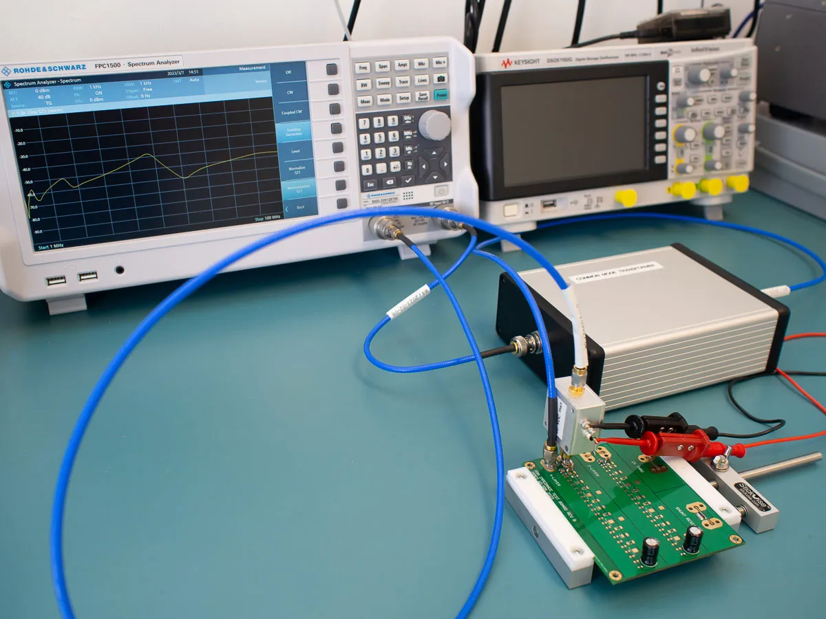
How to Perform PDN Impedance Measurement
Once a target is set, the next step is PDN impedance measurement to verify if your design meets the required specifications. Measurement is typically done using specialized equipment like a Vector Network Analyzer (VNA) or an oscilloscope with a low-noise probe. These tools help analyze the impedance profile across different frequencies, revealing potential issues like resonance peaks that could amplify noise.
To measure PDN impedance, follow these steps:
- Prepare the Setup: Connect the VNA to test points on the power rail, ensuring minimal interference from external noise sources.
- Measure Across Frequencies: Sweep from low frequencies (a few Hz) to high frequencies (up to 1GHz or more) to capture the full impedance profile.
- Analyze Results: Look for areas where impedance exceeds the target, especially at frequencies corresponding to switching speeds of your ICs (e.g., 100MHz for a high-speed processor).
Accurate measurement often requires a controlled environment to avoid parasitic effects from probes or test fixtures. If a resonance peak appears at 50MHz with an impedance of 100mΩ—far above the 5mΩ target—it indicates a need for design adjustments, such as adding decoupling capacitors.
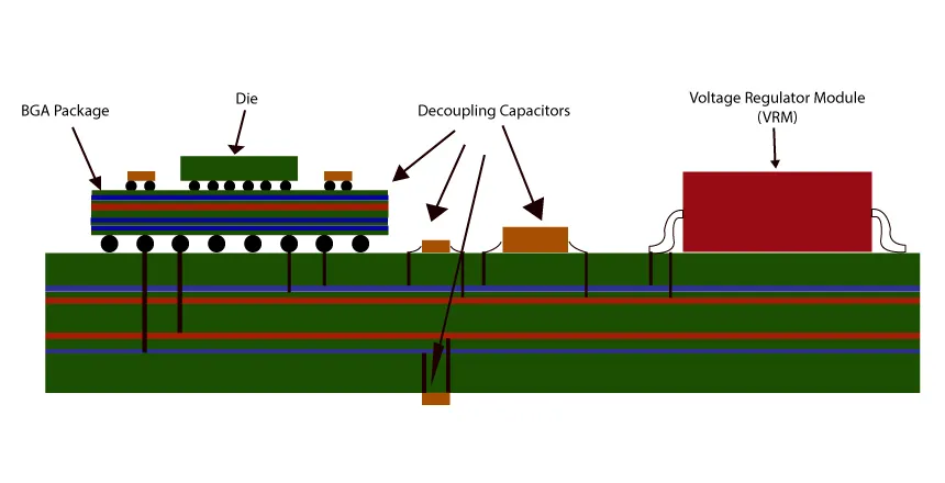
Designing a Low Impedance PDN: Key Strategies
A low impedance PDN is the foundation of good power integrity. The goal is to maintain impedance below the target across the entire frequency spectrum, minimizing voltage fluctuations and noise. Here are some proven strategies to achieve a low impedance PDN:
- Use Decoupling Capacitors: Place capacitors with different values (e.g., 0.1μF, 1μF, and 10μF) near power pins to handle transients at various frequencies. These capacitors act as local energy reservoirs, reducing impedance at high frequencies.
- Optimize Power Plane Design: Design power and ground planes as closely spaced layers (e.g., 5-10 mils apart) to create a low-inductance path. This can reduce impedance by up to 50% compared to wider spacing.
- Minimize Via Inductance: Use multiple vias for power connections to lower inductance. A single via might contribute 1nH of inductance, while four vias in parallel can reduce it to 0.25nH.
- Shorten Trace Lengths: Keep power traces as short as possible to reduce parasitic inductance and resistance, which directly impact impedance.
By combining these techniques, you can achieve a low impedance PDN that supports stable power delivery, even under demanding conditions like a 20A current surge.
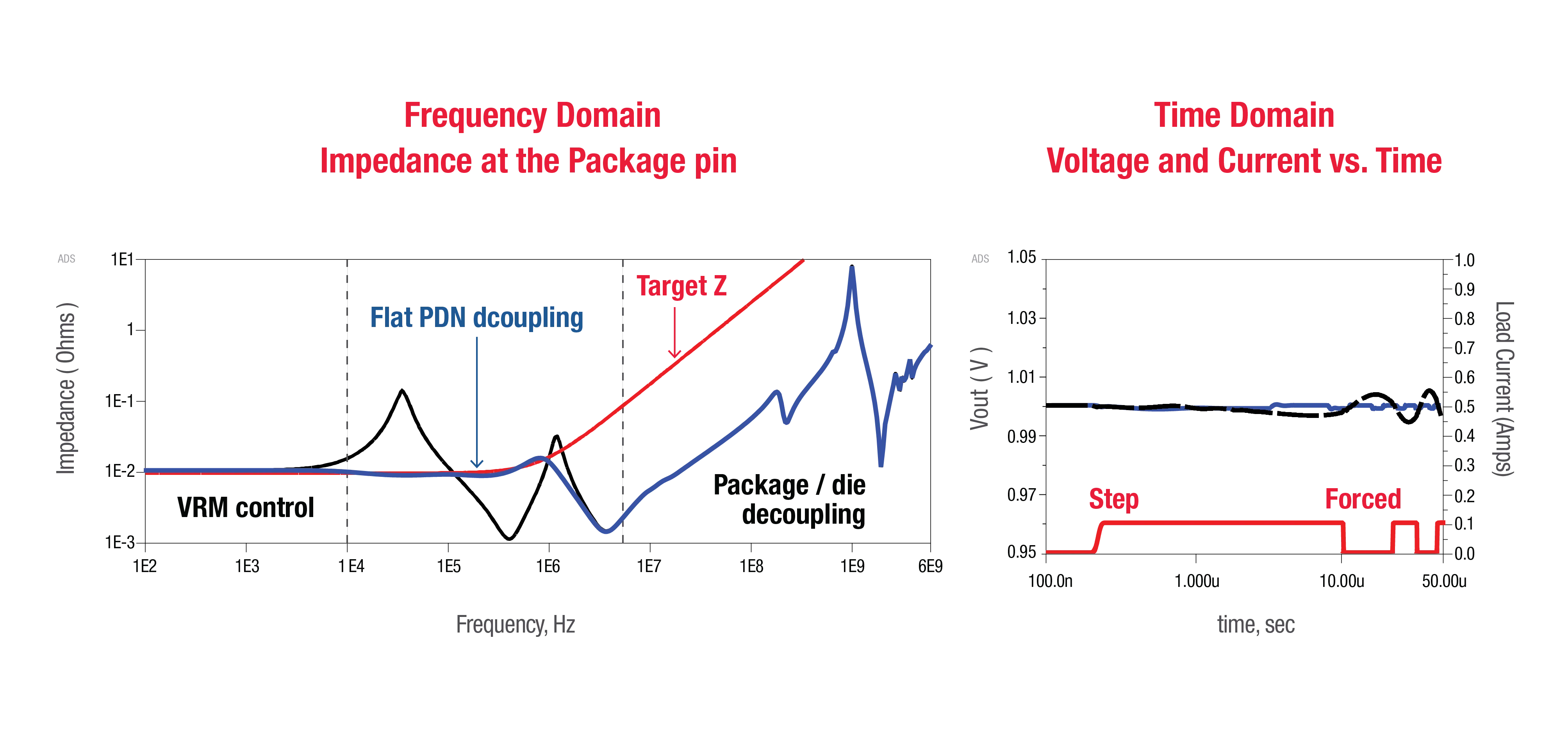
Running PDN Impedance Simulation for Design Validation
Before manufacturing a PCB, running a PDN impedance simulation is essential to predict performance and identify issues. Simulation tools allow you to model the PDN and analyze its impedance profile without building a physical prototype, saving time and cost.
Here’s how to approach PDN impedance simulation:
- Build a Model: Create a schematic or layout model of your PDN, including power planes, vias, capacitors, and IC power pins. Include parasitic elements like trace inductance (e.g., 0.5nH per inch) and capacitor ESL (Equivalent Series Inductance, often around 1nH).
- Set Frequency Range: Simulate from DC to several GHz to cover all relevant frequencies for your design.
- Analyze Impedance Curve: Look for peaks above the target impedance. For instance, a peak at 200MHz with 20mΩ impedance against a 5mΩ target indicates a resonance issue.
- Iterate Design: Adjust capacitor values or plane spacing in the simulation to flatten the impedance curve.
Simulation is a powerful way to validate your design early. Many engineers find that tweaking capacitor placement in simulation can reduce high-frequency impedance by 30-40%, avoiding costly redesigns after manufacturing.
PDN Impedance Optimization: Fine-Tuning for Power Integrity
PDN impedance optimization goes beyond initial design—it’s about fine-tuning to suppress noise and meet stringent performance goals. As chip sizes shrink and transistor counts increase (often exceeding 10 billion in modern ICs), power integrity challenges grow, making optimization critical.
Consider these optimization techniques:
- Multi-Layer Decoupling: Use a combination of bulk capacitors (100μF for low frequencies), mid-range capacitors (10μF for mid-frequencies), and small capacitors (0.1μF for high frequencies) to cover the full spectrum. This can reduce impedance peaks by up to 60% at critical frequencies.
- Anti-Resonance Management: Identify and suppress anti-resonance spikes—caused by interactions between capacitors and inductances—by adjusting capacitor values or adding damping resistors (e.g., 0.5Ω in series with a capacitor).
- Targeted Impedance Tuning: Focus on frequencies where your ICs are most active. For a 500MHz processor, prioritize low impedance around 500MHz and its harmonics (1GHz, 1.5GHz).
Optimization often involves a mix of simulation and measurement. For instance, after simulation reveals a 30mΩ peak at 100MHz, you might add a 1μF capacitor near the affected IC, then measure the real board to confirm the impedance drops to 5mΩ. This iterative process ensures the PDN meets all power integrity requirements.
Common Challenges in PDN Impedance Design and How to Overcome Them
Designing for PDN impedance isn’t without challenges. Here are some common issues and solutions:
- Resonance Peaks: These occur when capacitor and inductance interactions amplify impedance at specific frequencies. Solve by adjusting capacitor placement or adding damping elements.
- High-Frequency Noise: At frequencies above 1GHz, parasitic effects dominate. Use smaller capacitors (e.g., 0.01μF) with low ESL and place them as close as possible to power pins.
- Space Constraints: Modern designs often lack space for multiple capacitors. Prioritize high-impact locations near critical ICs and use embedded capacitance in multi-layer boards to save space.
Addressing these challenges requires a balance of theoretical knowledge, simulation, and real-world testing to ensure a robust PDN.
Conclusion: Building Better PCBs with PDN Impedance Mastery
Mastering PDN impedance is a cornerstone of effective power integrity design. By setting a clear PDN impedance target, conducting accurate PDN impedance measurement, designing a low impedance PDN, leveraging PDN impedance simulation, and focusing on PDN impedance optimization, you can ensure stable power delivery and minimize noise in your PCB designs. These steps are especially critical as devices become faster and more complex, demanding tighter control over voltage stability.
At ALLPCB, we’re committed to supporting engineers with resources and services to tackle power integrity challenges. Whether you’re working on a high-speed processor board or a compact IoT device, understanding and controlling PDN impedance will elevate your designs to the next level. Start applying these strategies in your next project to achieve reliable, high-performance results.


