ALLPCB


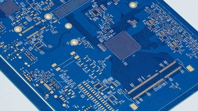
High-Density Interconnect (HDI) technology is a game-changer in the world of printed circuit boards (PCBs), enabling smaller, faster, and more efficient designs. However, HDI manufacturability and cost are critical concerns for engineers and designers aiming to balance performance with budget. In this comprehensive guide, we’ll explore how factors like materials, layers and laminations, vias in HDI classes, and optimal trace and space impact HDI PCB production and expenses. Whether you’re designing for consumer electronics or industrial applications, understanding these elements can help you achieve cost-effective and manufacturable HDI solutions.
What Influences HDI Manufacturability and Cost?
At its core, HDI manufacturability refers to how easily a design can be produced without errors or delays, while cost is tied to the resources, processes, and complexity involved. Key factors include the choice of materials, the number of layers and lamination cycles, the type and placement of vias, and the precision required for trace and space configurations. By optimizing these aspects, you can reduce production challenges and keep expenses in check. Let’s dive deeper into each of these areas to uncover practical strategies for efficient HDI PCB design.
1. Materials: The Foundation of HDI Manufacturability and Cost
The materials used in HDI PCBs play a significant role in both manufacturability and cost. Selecting the right substrate and laminate materials ensures that the board meets electrical, thermal, and mechanical requirements while remaining feasible to produce.
Substrate Choices and Cost Implications
Common materials for HDI boards include FR-4, high-frequency laminates, and advanced resin systems. Standard FR-4 is often the most cost-effective option, with prices ranging from $0.50 to $1.50 per square foot for basic grades, but it may not support high-speed signals above 5 GHz due to higher dielectric loss. High-frequency materials, such as PTFE-based laminates, can handle frequencies up to 10 GHz or more with lower signal loss (dielectric constant around 2.2-3.0), but they can cost 3-5 times more than FR-4. Choosing a material that balances performance with budget is crucial for cost control.
Thermal and Electrical Considerations
Materials must also withstand the thermal stress of multiple lamination cycles in HDI designs. For instance, a material with a glass transition temperature (Tg) of at least 170°C is recommended for boards undergoing 3-4 lamination cycles to prevent warping or delamination. Additionally, ensure the material’s dielectric constant and loss tangent align with your signal integrity needs. A mismatch can lead to impedance issues, requiring costly redesigns.
Tip for Manufacturability
Work closely with your fabrication partner to select materials that are readily available and compatible with their processes. Custom or exotic materials may increase lead times and costs by 20-30%, impacting overall project timelines.
2. Layers and Laminations: Balancing Complexity and Cost
HDI PCBs often require multiple layers to accommodate dense routing and compact designs. However, the number of layers and lamination cycles directly affects both manufacturability and cost.
Layer Count and Production Challenges
Each additional layer in an HDI board increases material usage and processing time. A 6-layer HDI board might cost around 30-50% more than a 4-layer board due to added materials and labor. Beyond 8 layers, costs can escalate further as alignment precision becomes critical, often requiring advanced equipment with tolerances as tight as ±0.002 inches for layer-to-layer registration.
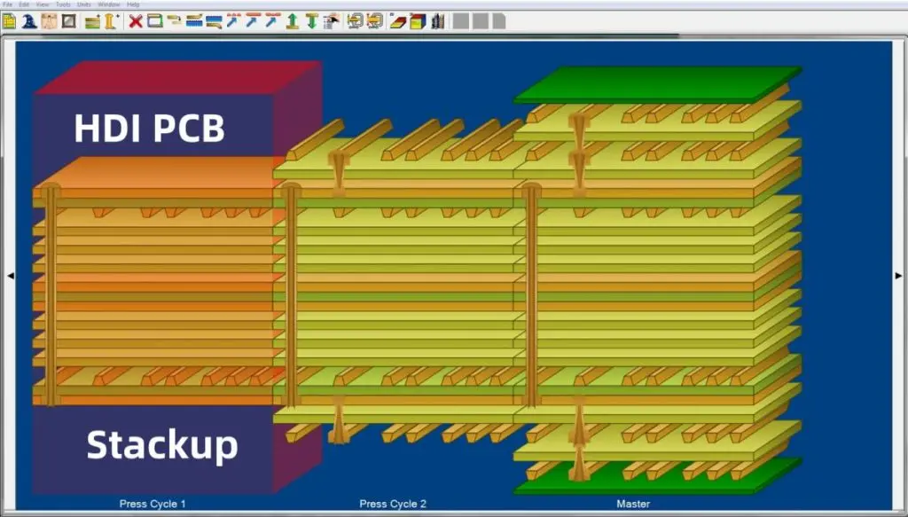
Sequential Lamination for HDI
HDI designs frequently use sequential lamination, where layers are built up in stages rather than all at once. This process allows for the integration of blind and buried vias but adds complexity. Each lamination cycle can increase production costs by 10-15% due to additional pressing and curing steps. To optimize manufacturability, minimize the number of lamination cycles by planning via structures early in the design phase.
Cost-Saving Strategy
If your design allows, consider reducing layer count by optimizing component placement and routing density. For example, using microvias instead of through-holes can free up space, potentially reducing the need for extra layers. This approach can save up to 20% on material and fabrication costs for complex designs.
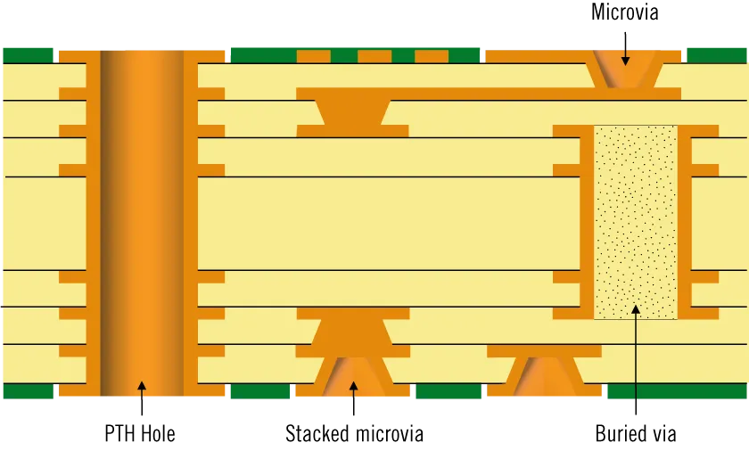
3. Vias in HDI Classes: Types, Challenges, and Cost Impact
Vias are a defining feature of HDI technology, enabling high-density routing by connecting different layers in a compact space. However, the type of via and its class significantly influence manufacturability and cost.
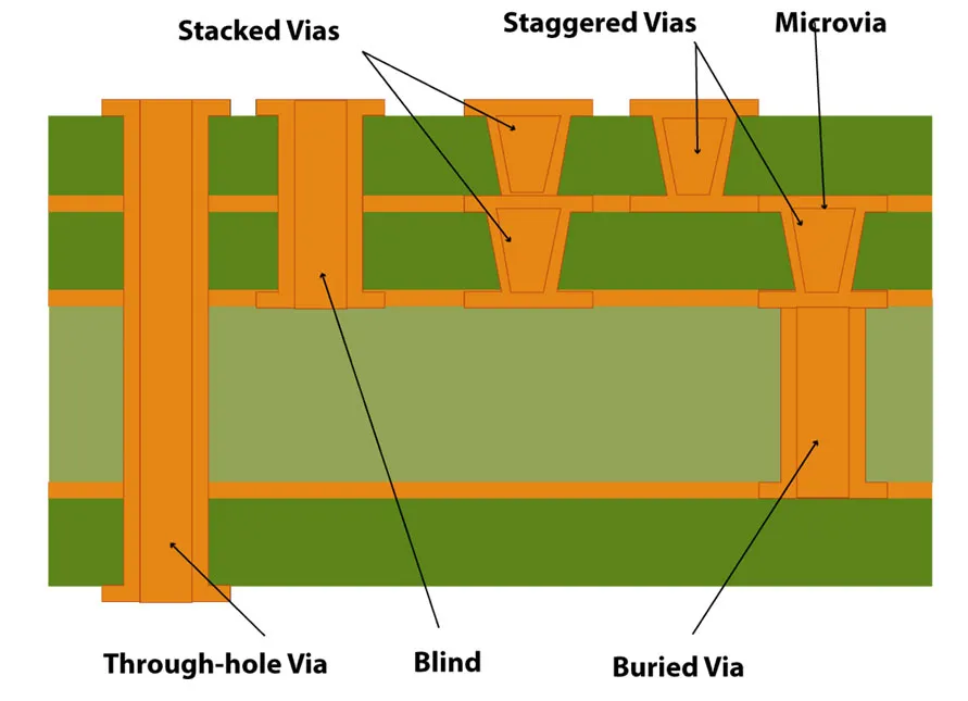
Types of Vias in HDI
HDI vias include blind vias (connecting an outer layer to an inner layer), buried vias (connecting inner layers only), and microvias (small-diameter vias, typically less than 0.006 inches). Microvias are often created using laser drilling, which offers precision but increases costs by 15-25% compared to mechanical drilling for through-holes. Blind and buried vias also require additional lamination steps, adding to production expenses.
HDI Via Classes and Standards
HDI designs are categorized into classes based on via density and manufacturing complexity, as defined by industry standards like IPC-2226. For instance, Type I HDI involves a single microvia layer on one or both sides of the core, which is relatively simple and cost-effective. Type III, with stacked microvias and multiple lamination cycles, can double the fabrication cost due to tighter tolerances (e.g., via aspect ratios of 0.8:1 or less) and increased risk of defects like via fill failures.
Manufacturability Tips for Vias
To improve manufacturability, avoid stacking more than two microvias without consulting your fabricator, as this can lead to reliability issues like cracking under thermal stress. Additionally, ensure via pads are large enough (typically 0.010-0.012 inches larger than the via diameter) to prevent drilling misalignment, which can cause yield losses of up to 10% in high-density designs.
Cost Optimization
Use the simplest via structure that meets your design needs. For example, opting for Type I or II HDI over Type III can reduce costs by 30-40% while still supporting moderate density requirements. Also, consider via-in-pad designs to save space, but be aware of the added cost for conductive or non-conductive fill, which can range from $0.10 to $0.50 per via.
4. Optimal Trace and Space: Precision for Performance and Cost
Trace width and spacing are critical in HDI designs, directly affecting signal integrity, manufacturability, and cost. Achieving optimal trace and space configurations requires balancing electrical performance with fabrication capabilities.
Trace Width and Spacing Standards
In HDI designs, trace widths often range from 0.003 to 0.005 inches, with spacing as tight as 0.003 inches to accommodate high-density routing. These fine lines demand advanced etching processes and tighter tolerances, increasing production costs by 20-30% compared to standard PCBs with 0.008-inch traces and spaces. For high-speed signals (e.g., above 1 GHz), maintaining controlled impedance (typically 50 ohms for single-ended signals) is essential, which may require precise trace geometries and dielectric thickness control.
Signal Integrity Considerations
Narrow traces and tight spacing can lead to crosstalk and signal loss if not designed properly. For instance, spacing below 0.003 inches may require additional shielding or ground planes to minimize interference, adding to layer count and cost. Simulation tools can help predict impedance and loss, ensuring traces are optimized before fabrication. A mismatch in impedance can result in signal reflections, degrading performance in applications like DDR4 memory interfaces operating at 2.4 GHz.
Manufacturability Challenges
Fabricating fine traces and spaces requires high-resolution imaging and etching equipment, which not all manufacturers have. Designs pushing below 0.003 inches for trace width or spacing may face yield issues, with defect rates increasing by 5-10% due to over-etching or shorts. To enhance manufacturability, adhere to your fabricator’s minimum trace and space capabilities, often listed as 0.004 inches for mid-range HDI processes.
Cost-Saving Tip
Relax trace and space constraints where high density isn’t critical. For non-critical areas, increasing trace width to 0.006 inches and spacing to 0.005 inches can lower fabrication costs by 10-15% while maintaining reliability. Additionally, route high-speed traces on outer layers when possible to avoid the added expense of buried signal layers.
5. Strategies to Optimize HDI Manufacturability and Reduce Costs
Balancing HDI manufacturability and cost requires a holistic approach to design and collaboration with your fabrication partner. Here are actionable strategies to streamline production and manage expenses:
Design for Manufacturability (DFM)
Incorporate DFM principles early in the design process. For example, avoid overly aggressive via stacking or trace densities that exceed your fabricator’s capabilities. Use design rule checks (DRC) to catch potential issues like insufficient annular rings (minimum 0.005 inches recommended) or misaligned vias before sending files for production. This can reduce costly revisions by up to 25%.
Collaborate with Fabricators
Engage with your manufacturing team during the design phase to align on material availability, via drilling capabilities, and layer stack-up options. Many fabricators offer free DFM reviews, which can identify cost drivers like unnecessary lamination cycles or incompatible materials, saving 10-20% on production costs.
Prototype and Test
Invest in small-scale prototypes to validate your HDI design before full production. Testing for signal integrity (e.g., ensuring impedance matches within ±10% of target) and thermal performance can prevent expensive failures in mass production. A single prototype run costing $500-$1000 can save thousands in rework costs.
Standardize Where Possible
Stick to standard materials, via sizes (e.g., 0.004-inch microvias), and layer counts that align with common manufacturing processes. Customization often leads to higher costs—up to 50% more for non-standard designs—due to specialized equipment or extended lead times.
Conclusion: Mastering HDI Manufacturability and Cost
HDI technology offers unparalleled advantages for compact, high-performance electronics, but achieving manufacturability while controlling costs demands careful planning. By focusing on the right materials, optimizing layers and laminations, selecting appropriate vias for HDI classes, and designing with optimal trace and space configurations, you can create efficient and budget-friendly HDI PCBs. Remember to leverage DFM practices and collaborate with your fabrication partner to address potential challenges early. With these strategies, you’ll be well-equipped to tackle the complexities of HDI design and bring your innovative projects to life without breaking the bank.