ALLPCB


In the world of printed circuit board (PCB) design and manufacturing, engineers often face a critical decision: Should they prioritize technologies like flexible PCBs (Flex) for enhanced product reliability, or opt for advanced via structures like blind and buried vias to reduce fabrication costs? While both approaches have their unique advantages, determining which is more "normal" or commonly used depends on the specific needs of a project. In this blog, we’ll dive deep into the characteristics of Flex PCBs and blind and buried vias, comparing their impact on reliability, cost, and manufacturing processes. By the end, you’ll have a clear understanding of which technology might suit your design goals.
At a high level, Flex PCBs are often favored in applications requiring durability and adaptability, such as wearable devices or compact electronics, due to their ability to bend without breaking. On the other hand, blind and buried vias are more common in high-density designs where space and cost efficiency are critical, as they allow for compact layouts without increasing board size. Let’s explore these technologies in detail to help you make an informed choice for your next project.
What Are Flex PCBs and How Do They Boost Reliability?
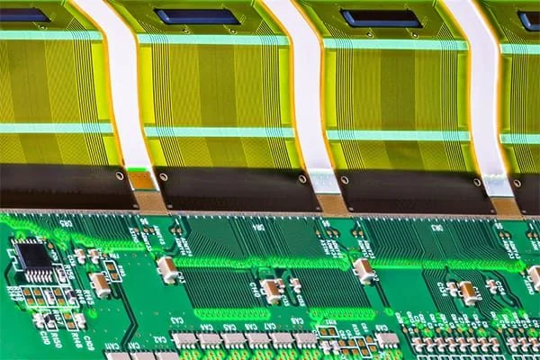
Flex PCBs, or flexible printed circuit boards, are designed using materials like polyimide that allow the board to bend and twist without damaging the circuitry. This flexibility makes them ideal for applications where space is limited or where the board must conform to a specific shape, such as in medical devices, automotive systems, and consumer electronics like smartphones.
One of the primary benefits of Flex PCBs is their enhanced reliability. Traditional rigid PCBs can crack or fail under mechanical stress, especially in environments with vibration or constant movement. Flex PCBs, however, can withstand bending cycles—often up to 200,000 cycles or more—without losing electrical performance. This durability translates to longer product lifespans and fewer failures in the field. For instance, in automotive applications, Flex PCBs are often used in dashboard controls, where they endure constant vibrations and temperature fluctuations.
Additionally, Flex PCBs reduce the need for connectors and cables, which are common points of failure in electronic assemblies. By integrating circuits directly into a flexible substrate, the design minimizes potential weak spots, further improving reliability. However, this comes at a trade-off: Flex PCBs typically have a higher initial manufacturing cost due to specialized materials and processes.
Understanding Blind and Buried Vias in PCB Design
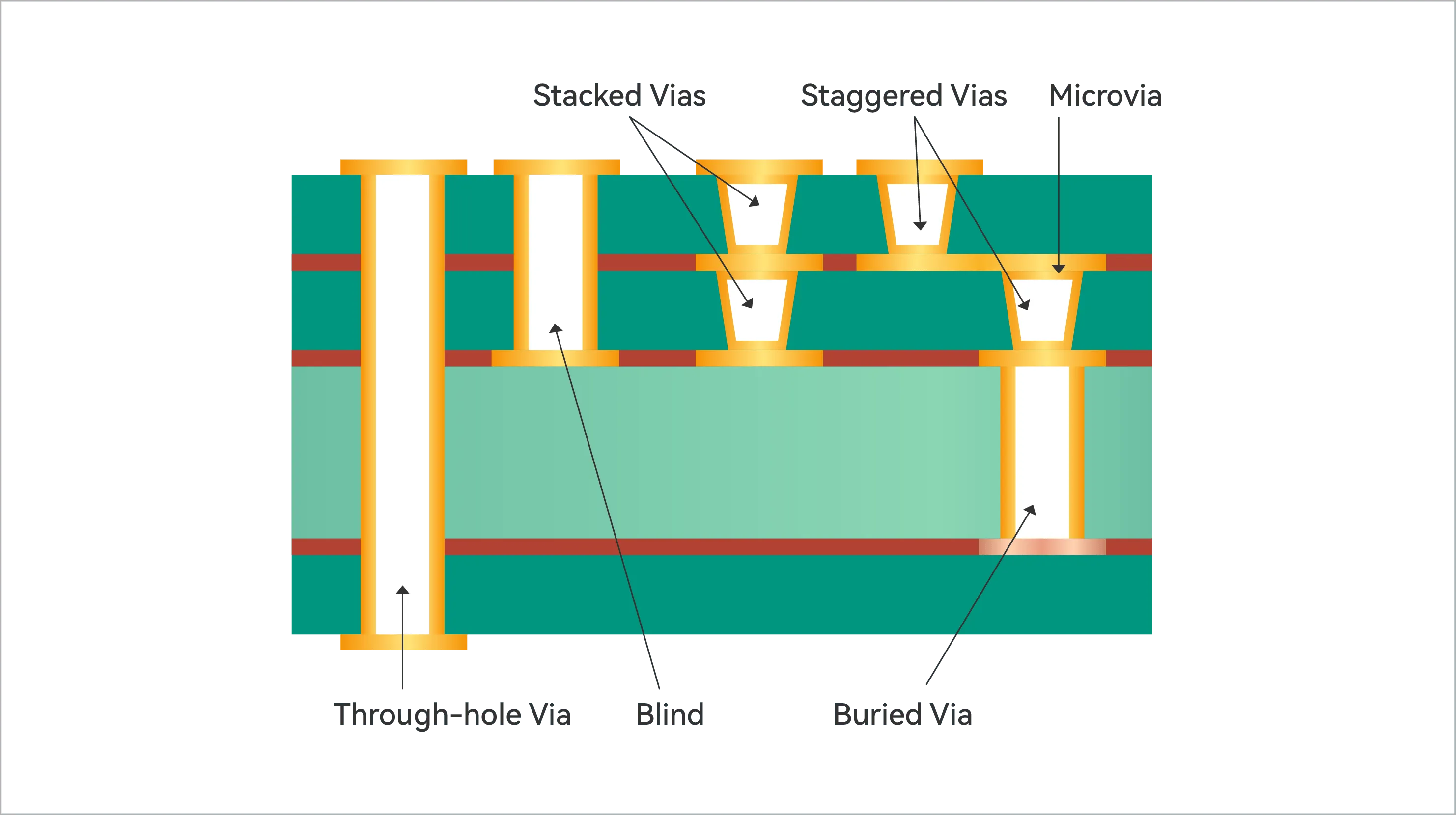
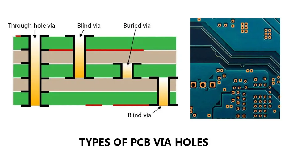
Blind and buried vias are advanced interconnect technologies used in multilayer PCBs to optimize space and performance. Unlike traditional through-hole vias that pass through the entire board, blind vias connect an outer layer to an inner layer without penetrating the full thickness of the board. Buried vias, on the other hand, are completely enclosed within the inner layers, invisible from the board’s surface.
These via types are particularly useful in high-density interconnect (HDI) designs, where space is at a premium. By eliminating the need for vias to pass through unnecessary layers, blind and buried vias free up surface area for additional components or traces. This can significantly reduce the overall size of the PCB, making them a popular choice in compact devices like smartphones and tablets.
From a cost perspective, blind and buried vias can reduce fabrication expenses in certain scenarios. By allowing for smaller board sizes, they decrease material usage, which can lower costs, especially in large production runs. However, the manufacturing process for these vias is more complex, often involving laser drilling for microvias (small vias with diameters around 3-6 mils). This complexity can increase upfront costs, particularly for prototypes or low-volume production.
Comparing Product Reliability: Flex PCBs vs. Blind and Buried Vias
When it comes to product reliability, Flex PCBs generally have the upper hand. Their ability to withstand mechanical stress, vibrations, and thermal expansion makes them a go-to choice for applications where durability is critical. For example, in aerospace systems, Flex PCBs are often used in tight spaces where rigid boards would fail under constant movement or extreme conditions.
Blind and buried vias, while effective for space optimization, do not inherently improve reliability in the same way. In fact, their use can introduce reliability concerns if not designed or manufactured properly. For instance, poorly drilled blind vias can lead to incomplete connections, resulting in signal integrity issues. Additionally, the smaller size of microvias (often used in HDI designs with blind and buried vias) can make them more susceptible to cracking under thermal stress, especially if the aspect ratio (depth to diameter) exceeds recommended limits, such as 1:1 for microvias.
That said, when implemented correctly, blind and buried vias can indirectly enhance reliability by enabling better signal integrity. By shortening trace lengths and reducing parasitic capacitance, these vias can improve electrical performance, which is crucial for high-speed applications operating at frequencies above 1 GHz. So, while Flex PCBs excel in mechanical reliability, blind and buried vias can contribute to electrical reliability when used in the right context.
Cost Analysis: Fabrication Savings with Blind and Buried Vias vs. Flex PCBs
Cost is often a deciding factor in PCB design, and here, blind and buried vias can offer advantages over Flex PCBs in specific scenarios. The ability to reduce board size with blind and buried vias directly translates to lower material costs. For instance, a smaller board might reduce the required laminate area by 20-30%, depending on the design, leading to significant savings in high-volume production.
However, the manufacturing process for blind and buried vias adds complexity. Laser drilling, sequential lamination, and precise alignment during fabrication increase production time and cost, especially for prototypes. In contrast, once the design is finalized, the per-unit cost in mass production often drops, making this approach more economical for large runs.
Flex PCBs, by comparison, typically have a higher baseline cost due to the specialized materials and manufacturing techniques required. The flexible substrates, such as polyimide, are more expensive than standard FR-4 materials used in rigid PCBs. Moreover, the design process for Flex PCBs often requires additional considerations, like ensuring proper bend radii (typically at least 10 times the board thickness) to avoid stress fractures, which can further increase design and testing costs.
In summary, if cost reduction is the primary goal and the project involves high-density designs with large production volumes, blind and buried vias may offer a more cost-effective solution. For smaller runs or applications prioritizing durability over compactness, the higher cost of Flex PCBs might be justified.
Manufacturing Challenges and Considerations
Both Flex PCBs and blind/buried vias come with unique manufacturing challenges that can impact project timelines and costs. For Flex PCBs, the manufacturing process requires specialized equipment to handle flexible materials without causing damage. The assembly process can also be more complex, as components must be placed and soldered on a non-rigid surface, sometimes requiring custom fixtures to hold the board in place.
Blind and buried vias, meanwhile, demand precision in drilling and lamination. Laser-drilled microvias, often used for blind vias, require tight control over parameters like laser power and pulse duration to avoid damaging surrounding materials. Misalignment during sequential lamination can also lead to defective boards, increasing scrap rates if not managed carefully. As a result, working with an experienced manufacturer is crucial to ensure quality when using these advanced via technologies.
From a design perspective, engineers must also consider the impact on signal integrity and thermal management. For Flex PCBs, signal speeds can be slightly slower due to the dielectric properties of flexible materials, with dielectric constants often around 3.2-3.5 compared to 4.0-4.5 for standard FR-4. For blind and buried vias, impedance mismatches can occur if the via transitions are not carefully designed, potentially affecting high-speed signals above 5 GHz.
Which Is More "Normal" in Today’s Industry?
Determining which technology is more "normal" or widely used depends on the industry and application. Blind and buried vias are increasingly common in consumer electronics, where the push for smaller, lighter devices drives the adoption of HDI designs. These vias are a staple in products like smartphones, tablets, and laptops, where board space is at a premium and production volumes are high, justifying the initial investment in complex manufacturing processes.
Flex PCBs, while not as ubiquitous as HDI designs with blind and buried vias, are the standard in applications where flexibility and reliability are non-negotiable. Industries like medical, automotive, and aerospace rely heavily on Flex PCBs for their ability to fit into tight spaces and endure harsh conditions. However, their higher cost often limits their use to specialized applications rather than mass-market products.
In terms of sheer volume, blind and buried vias are likely more "normal" due to their widespread use in high-density consumer electronics. However, the choice ultimately hinges on the specific requirements of your project. If reliability under mechanical stress is critical, Flex PCBs are the better fit. If cost and space savings are the priority, blind and buried vias are the way to go.
Practical Tips for Choosing the Right Technology
To help you decide between Flex PCBs and blind/buried vias, consider the following factors:
- Application Environment: Will the PCB be subjected to bending, vibration, or extreme conditions? If yes, opt for Flex PCBs for superior mechanical reliability.
- Space Constraints: If minimizing board size is crucial, blind and buried vias can help create a more compact design.
- Production Volume: For high-volume runs, the cost savings from smaller boards with blind and buried vias often outweigh the initial setup costs. For low-volume or prototype runs, Flex PCBs might be more feasible despite their higher cost.
- Signal Requirements: High-speed designs may benefit from the shorter trace lengths enabled by blind and buried vias, improving signal integrity.
Collaborating with your manufacturing partner early in the design process can also help optimize for cost and reliability. They can provide insights into material selection, stackup design, and process limitations, ensuring your chosen technology aligns with your project goals.
Conclusion: Balancing Reliability, Cost, and Design Needs
In the debate between Flex PCBs for enhanced product reliability and blind/buried vias for potential cost reduction in manufacturing, there is no one-size-fits-all answer. Flex PCBs shine in applications where durability and adaptability are paramount, offering unmatched reliability in challenging environments. Blind and buried vias, however, are often the more "normal" choice in today’s high-density electronics, providing space and cost savings that are critical for mass production.
By carefully evaluating your project’s requirements—whether it’s mechanical reliability, electrical performance, or budget constraints—you can select the technology that best meets your needs. Whether you prioritize the flexibility of Flex PCBs or the compactness of designs with blind and buried vias, working with a trusted manufacturing partner ensures a smooth transition from design to production.