ALLPCB


1. Why is EMC Design Necessary?
Proper electromagnetic compatibility (EMC) design is crucial for several reasons. It ensures the product meets its functional requirements, reduces debugging time, and guarantees compliance with EMC standards. A well-designed product will not cause electromagnetic interference (EMI) with other devices in its operating environment.
2. Key Areas of EMC Design
EMC design encompasses multiple aspects of product development, including:
- Circuit design (including component selection)
- Software design
- Printed circuit board (PCB) layout
- Shielding and enclosure design
- Signal and power line filtering
- Circuit grounding strategy
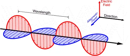
3. The Use of Decibels (dB) in EMC
Decibels are used in EMC because they provide a logarithmic scale for representing values. This is ideal for describing the wide amplitude and frequency ranges encountered in EMC testing, making it easier to visualize and analyze data on a graph.
4. Foundational Knowledge for EMC Excellence
To become proficient in EMC, an engineer should focus on the following foundational areas:
- EMC Standards: Familiarize yourself with key standards like EN 55022 (GB 9254) and EN 55024, along with basic testing principles.
- EMI Components: Understand the application of EMI suppression components such as capacitors, ferrite beads, differential mode chokes, and common mode chokes.
- PCB Layout: Master the principles of PCB layout for EMC, including stack-up design, component placement, and high-speed routing rules.
- Troubleshooting: Develop a systematic approach to analyzing and resolving EMC issues when they arise.
These skills are essential for any modern hardware engineer.
5. Essential Knowledge for PCB Design
A successful PCB designer should master the following:
- Proficiency in PCB design software (e.g., PowerPCB, Cadence).
- A deep understanding of the product architecture and schematic circuit principles, including both digital and analog circuits.
- Knowledge of PCB manufacturing processes, capabilities, and design for manufacturability (DFM).
- Expertise in high-speed design topics, including signal integrity (SI), power integrity (PI), simulation, and EMC (both EMI and EMS).
- For radio frequency (RF) applications, a solid understanding of RF principles is required.
- Knowledge of safety standards (e.g., GB4943 or UL60950) to determine required insulation and clearance distances, which can typically be found in reference tables.
6. Basic Principles of EMC in Circuit Design
Designers often focus on product functionality without integrating EMC considerations, leading to functional and other forms of interference. Effective EMC design in electronic circuits should start at the component level.
Component Selection Rules:
- For high-frequency filtering, prefer feed-through or stand-off capacitors with low lead inductance over leaded capacitors.
- When using leaded capacitors, account for the effect of lead inductance on filtering efficiency.
- Aluminum electrolytic capacitors can experience transient dielectric breakdown. In circuits with high ripple or voltage transients, use solid-state capacitors instead.
- Use resistors with low parasitic inductance and capacitance. Chip resistors are suitable for ultra-high-frequency bands.
- Instead of a single-stage filter with a large inductor (which has high parasitic capacitance), use a multi-stage filter with smaller inductors to improve insertion loss at low frequencies.
- Be aware of the saturation characteristics of magnetic core inductors. High-level pulses can reduce inductance and degrade filter insertion loss.
- Use shielded relays whenever possible and connect the shield to ground.
- Select effectively shielded and isolated input transformers.
- Power transformers for sensitive circuits should have an electrostatic shield, with both the shield and transformer case grounded.
- Use shielded cables for internal interconnects to prevent interference coupling.
- Choose connectors with a sufficient number of pins to ensure each shield is connected to its respective pin.
7. Troubleshooting Common EMC Issues
Square Wave Driving an Inductive Sensor
- Perform signal testing in a shielded environment. If this is not possible, at least shield the sensor and its preamplifier.
- Use differential probes for testing, or at least keep the probe's ground lead as short as possible to minimize measurement error.
- Your circuit's operating frequency is not excessively high. Ringing can be reduced through careful layout. For better noise performance, consider common-mode signal rejection and insert a common-mode choke if necessary. Also, be mindful of noise from switching power supplies and avoid power supply coupling.
- If the sensor allows, use a current amplification mode to improve speed and reduce noise. Place the analog switch after the preamplifier; although this adds a pre-amp stage, it significantly improves performance and simplifies debugging.
- If waveform integrity is critical, consider adding frequency compensation. If only digital detection is needed, lower the operating frequency. In general, use the lowest possible frequency and DC-block where feasible.
- Pay attention to anti-aliasing filters before the ADC and use software filtering to improve data stability.
GPS Interference in Portable Media Players (PMPs)
Problem: In a PMP with MP3/MP4, FM, and GPS functions, the internal GPS antenna is susceptible to EMI from the MCU, SDRAM, and crystal oscillators, which degrades satellite reception and positioning performance.
Solution: Place an ESD filter on the signal lines. These components provide both electrostatic discharge protection and EMI filtering. This method is used in mobile phones with GPS functionality. Components are available from manufacturers such as TE Connectivity (Raychem), Inpaq, and ICT.
DC Motor Speed Control Circuit Noise
Problem: A speed control circuit for a DC permanent magnet motor shows excessive radiation (over 12 dB) between 30-50 MHz, even after attempting a PI filter (0.33uF cap + inductor + 0.33uF cap) and adding four series inductors on the power input.
Solution: Generally, LC or Pi-type filters are more effective than single capacitors or inductors. The issue might be that the feedback noise from the DC motor is high-amplitude and low-frequency. This requires a larger inductance value for effective filtering. Try using a multi-stage capacitor filter in combination with a larger inductor.
Electrostatic Discharge (ESD) Test Failure
Problem: A device with a metal decorative trim passes a 4kV contact discharge test but fails an 8kV air discharge test, causing the 32kHz crystal to stop oscillating.
Solution: With metal parts present, the effects of air and contact discharge are similar. Try applying an insulating coating or paint to the metal frame to mitigate the discharge path.
Radiation from a Mobile Phone Charger
Problem: A new mobile phone fails CCC certification due to a radiation spike of +5 dB in the 50-60 MHz range, likely caused by the charger. The phone's circuit only contains a few decoupling capacitors (1uF, 100uF).
Solution (without modifying the charger): The issue is likely related to the battery and charging circuit. Try adjusting capacitor values (increasing larger ones, decreasing smaller ones) and adding a ferrite bead in series. Additionally, grounding and shielding the switching inductor's casing may help.
8. Advanced EMC and PCB Design Topics
Understanding Differential Signals
- Definition: A differential signal uses two complementary traces to transmit a single signal, with the receiver interpreting the voltage difference between them. This technique can be used for both analog and digital signals.
- Frequency Response: A differential pair is a four-port network that can be analyzed in both differential and common modes. To analyze its frequency response, you must apply a common-mode source (same polarity) and a differential-mode source (opposite polarity) and measure the resulting common-mode voltage Vcm = (V1+V2)/2 and differential-mode voltage Vdm = V1-V2.
- Conversion to Single-Ended: Differential signals are typically converted to single-ended signals using a differential amplifier. A key performance metric for these amplifiers is the Common-Mode Rejection Ratio (CMRR), which measures how well the amplifier rejects noise common to both signal lines.
Using Simulation for EMC Analysis
- Simulation vs. Testing: While no simulation tool can replace physical testing, simulators like Ansys SIwave (for PCB) and HFSS (for 3D structures) can effectively model near-field and far-field radiation. The accuracy of the simulation depends on correctly identifying potential EMI sources (e.g., differential vs. common-mode radiation, current vs. voltage sources) and configuring the software accordingly.
- Frequency Range: Ansys tools can simulate from DC to tens of GHz. While tools like HyperLynx are effective for SI and crosstalk analysis, comprehensive EMC analysis requires considering power plane noise, decoupling strategies, and current distribution, all of which can be modeled in tools like SIwave. These tools are compatible with exports from layout software like Mentor PADS.
- Boundary Conditions: Lumped resistors can be modeled using RLC boundaries. Thin-film resistors can be modeled using surface impedance or impedance boundaries.
Ground and Power Plane Design
- Ground Plane Splitting: Splitting a ground plane is done to isolate a noise source from a sensitive circuit (e.g., digital ground from analog ground). However, this can create signal integrity issues if a trace must cross the split. Simulation tools can help analyze the isolation between different points on the plane. Other methods to improve isolation include layering, decoupling, and single-point grounding.
- Capacitor Across Power Splits: A capacitor placed across two different power planes provides a low-impedance path for high-frequency return currents. While the main DC power is filtered, digital circuits themselves generate high-frequency AC noise as transistors switch. This capacitor provides a local source of charge to meet instantaneous current demands, creating a local AC current loop and stabilizing the power rail.
- PCB to Chassis Grounding: The principle is to provide a low-impedance path for return currents and control their flow. For example, connecting the PCB ground to the chassis ground near high-frequency components or clock generators using mounting screws minimizes the current loop area and reduces electromagnetic radiation.
High-Speed, High-Density PCB Design
In high-density designs, crosstalk is a major concern affecting timing and signal integrity. Key techniques include:
- Maintain continuous and matched characteristic impedance for traces.
- Ensure adequate trace spacing (a common rule is 2x the trace width). Use simulation to determine the minimum acceptable spacing.
- Select appropriate termination schemes.
- Avoid running traces parallel to each other on adjacent layers, as this creates stronger coupling than side-by-side traces on the same layer.
- Use blind and buried vias to increase routing area, though this increases manufacturing cost.
While achieving perfect parallelism and length matching is difficult, it should be a design goal. Adding pads for optional termination components can also help mitigate SI issues.
Filtering on Analog Power Rails
LC vs. RC Filters: An LC filter may perform worse than an RC filter if the inductor value is too small for the noise frequency being targeted. The reactance of an inductor is frequency-dependent. However, RC filters dissipate power in the resistor, reducing efficiency. The choice depends on the noise profile, efficiency requirements, and transient current demands. A large inductor can impede the delivery of instantaneous current, increasing ripple noise.
Choosing L and C Values: The inductor value depends on the noise frequency and the circuit's transient current needs. The capacitor value is determined by the allowable ripple noise specification; lower ripple requires a larger capacitance. The capacitor's ESR and ESL are also important factors. If the LC filter is at the output of a switching regulator, its pole-zero characteristics must be considered to ensure the stability of the feedback loop.
Balancing Signal Integrity and EMI
To achieve a balance between SI and EMI, the most effective method is often to reduce communication speed or signal slew rates, but this is not always a viable option. Careful design focusing on impedance control, clean return paths, and proper termination is key.
Cost-Effective EMC on PCBs
EMC-related costs on a PCB often come from adding ground layers for shielding or using components like ferrite beads and chokes. To minimize costs while meeting EMC requirements:
- Use components with slower slew rates to reduce high-frequency harmonics.
- Position high-frequency components away from external connectors.
- Ensure proper impedance matching and a clean return current path for high-speed signals.
- Place adequate decoupling capacitors near the power pins of each IC.
- Consider splitting the ground plane near external connectors and connecting the connector ground directly to the chassis ground.
- Use guard traces next to very high-speed signals where necessary.
- Pull the power plane in from the edge of the ground plane by a distance of 20H (where H is the distance between the planes).
Avoiding High-Frequency Interference and Crosstalk
- General Interference: The primary goal is to reduce the electromagnetic field from high-frequency signals. This can be done by increasing the distance between high-speed digital signals and sensitive analog signals or by adding a grounded guard trace alongside the analog signal.
- Crosstalk: Crosstalk occurs during signal transitions and is proportional to the signal's slew rate (di/dt). It consists of forward and backward components. On a PCB transmission line, the forward crosstalk from capacitive and inductive coupling tends to cancel out, while the backward crosstalk components add up. Analysis modes include default, tri-state, and worst-case to evaluate the impact of crosstalk.
- Clock Line Shielding: Whether to add shield ground lines on both sides of a clock trace depends on the specific crosstalk and EMI analysis of the board. Improperly implemented shield traces can sometimes worsen the problem.
System-Level Grounding
- Inter-Board Grounding: When multiple PCBs are connected, there must be an adequate return path for current. The current will follow the path of least impedance. Ensure a sufficient number of ground pins in the connectors between boards to keep this impedance low and minimize ground noise.
- Ground Loops: To reduce interference, minimize the area of current loops. For ground connections, it is generally better to use a tree-like or star grounding structure rather than creating closed loops. Also, maximize the area of the ground plane wherever possible.
- Ground Partitioning (Digital, Analog, Protective): Grounds are partitioned primarily for EMC reasons. The goal is to prevent noise from digital circuits from interfering with sensitive analog circuits via conduction. A protective ground is used for ESD safety, providing a separate path for static discharge to flow to the chassis or earth ground, similar to a lightning rod. Regardless of how many types of grounds are defined on the PCB, they all ultimately connect to a single system ground.
Copper Pour on PCBs
Copper pours are used for several reasons:
- EMC: A large ground or power pour acts as a shield. Specialized pours like a protective ground (PGND) can offer protection from external events.
- Manufacturing: On sparse layers, copper pours help ensure uniform plating during manufacturing and prevent board warping during lamination.
- Signal Integrity: Provides a continuous return path for high-frequency digital signals and reduces the need for routed DC power nets.
- Other: Copper pours are also used for thermal dissipation and as mounting pads for special components.
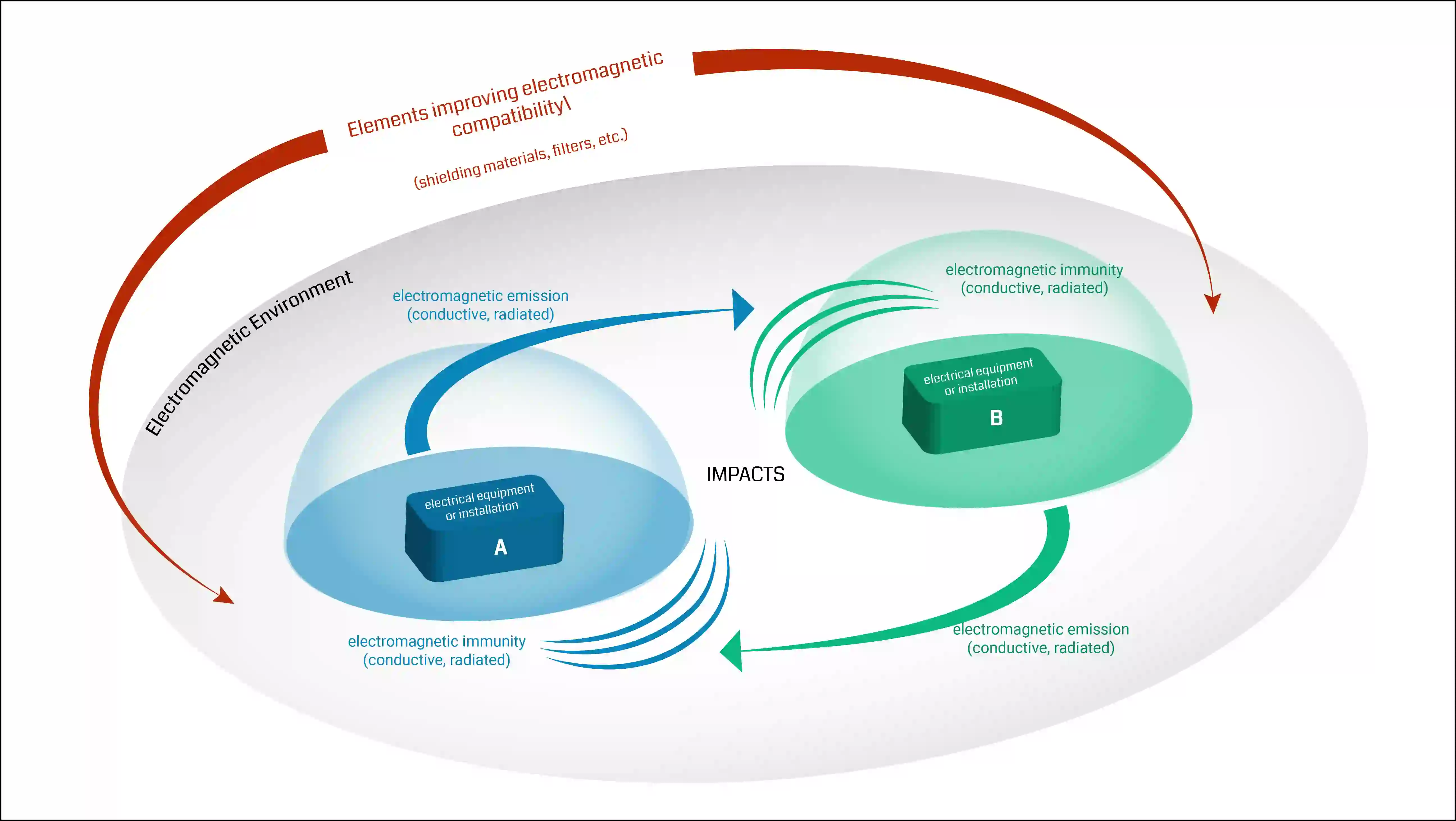
FCC and EMC Definitions
- FCC: Federal Communications Commission, a US regulatory agency that sets standards for electronic devices.
- EMC: Electromagnetic Compatibility, a characteristic of an electronic device ensuring it does not cause or suffer from undue electromagnetic interference.