ALLPCB


Grounding is one of the most critical aspects of designing a printed circuit board (PCB). Poor grounding can lead to noise, interference, and unreliable performance, while effective grounding ensures signal integrity and reduces electromagnetic interference (EMI). If you're new to PCB design, understanding grounding strategies like single point grounding, multi-point grounding, ground planes, and more can make a huge difference in your projects. In this beginner's guide, we'll break down the essentials of PCB grounding and provide actionable tips to help you create quieter, more efficient layouts.
This comprehensive guide will walk you through various grounding techniques, including single point grounding, multi-point grounding, ground planes, star grounding, split ground planes, chassis ground, digital ground, and analog ground. By the end, you'll have a solid foundation to apply these strategies in your designs and avoid common pitfalls.
Why PCB Grounding Matters in Your Design
Grounding in PCB design serves as a reference point for all signals and power in your circuit. It provides a low-impedance path for return currents, helps stabilize voltages, and shields against noise and interference. Without proper grounding, you might face issues like crosstalk, signal distortion, or even complete circuit failure. For instance, high-frequency signals can generate EMI if return paths are not well-defined, potentially disrupting nearby components.
Effective PCB grounding minimizes these risks by ensuring that currents flow predictably and noise is kept in check. Whether you're working on a simple hobby project or a complex mixed-signal system, grounding is a non-negotiable step for reliable performance.
Key Grounding Concepts for Beginners
Before diving into specific strategies, let's cover some fundamental grounding concepts. Grounding isn't just about connecting everything to a single point; it involves understanding how currents flow and how different parts of your circuit interact.
- Return Path: Every signal in your PCB has a return current that must flow back to its source. A good grounding strategy ensures this path is short and direct to avoid noise.
- Ground Loop: This happens when there are multiple paths for return currents, creating loops that can pick up interference. Minimizing ground loops is a key goal in grounding design.
- Impedance: Ground connections should have low impedance to prevent voltage drops. For high-frequency signals, even a small impedance (like 0.1 ohms) can cause significant issues.
With these basics in mind, let's explore specific PCB grounding strategies that you can apply to your designs.
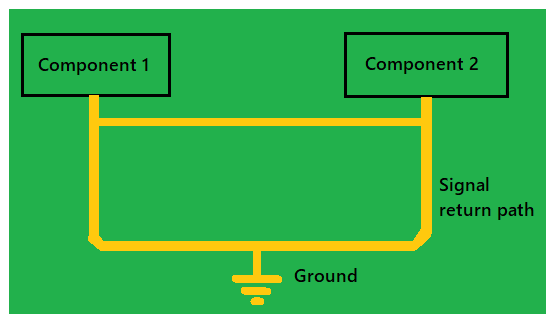
Single Point Grounding: Keeping It Simple
Single point grounding is one of the simplest and most effective grounding strategies for beginners. In this approach, all ground connections in the circuit are tied to a single common point. This minimizes the risk of ground loops since there's only one path for return currents to follow.
This method works best for low-frequency circuits or small designs where signal speeds are below 1 MHz. For example, in a basic audio amplifier circuit, connecting all grounds to a single point near the power supply can prevent hum and noise from interfering with the audio signal.
However, single point grounding has limitations. As circuit complexity or frequency increases, this method can lead to long return paths, increasing impedance and noise. Use this strategy for simple projects, but consider other approaches for more advanced designs.
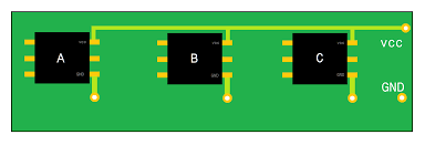
Multi-Point Grounding: Handling Higher Frequencies
Multi-point grounding connects different parts of the circuit to the ground at multiple locations, usually through a ground plane. This approach is ideal for high-frequency designs (above 10 MHz) because it shortens return paths and reduces impedance. By providing multiple ground connections, you ensure that return currents can flow directly to the nearest ground point, minimizing noise.
For instance, in a high-speed digital circuit like a microcontroller board, multi-point grounding helps manage fast-switching signals that could otherwise generate EMI. The key is to use a solid ground plane to tie these points together, which we'll discuss next.
While effective, multi-point grounding requires careful planning to avoid creating ground loops. Ensure that all ground points are connected through a low-impedance path to maintain signal integrity.
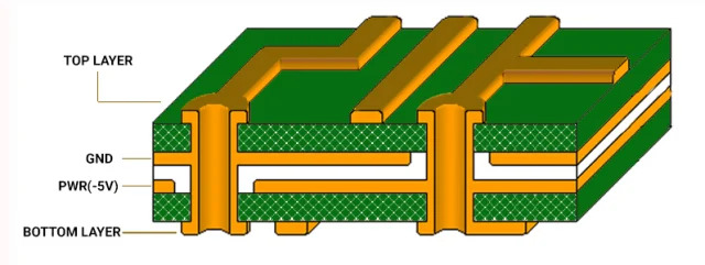
Ground Planes: The Backbone of Modern PCB Grounding
A ground plane is a large, continuous layer of copper on your PCB dedicated to grounding. It acts as a low-impedance reference for all signals and provides a direct return path for currents. Ground planes are essential in multi-layer PCBs and high-speed designs because they reduce noise and EMI significantly.
For example, in a 4-layer PCB, one layer is often dedicated entirely to the ground plane. This setup ensures that signals on adjacent layers have a nearby return path, keeping impedance low (often below 0.01 ohms at high frequencies). Ground planes also help with heat dissipation, which is a bonus for power-heavy designs.
When using ground planes, place vias strategically to connect components to the ground layer. Avoid splitting the plane unnecessarily, as this can disrupt return paths and create noise.
Star Grounding: A Hybrid Approach
Star grounding combines elements of single point grounding with a structured layout. In this method, different sections of the circuit (like power, analog, and digital) are connected to a central ground point in a star-like pattern. Each section has its own ground path leading to the center, reducing the chance of noise coupling between different parts of the circuit.
This strategy is particularly useful for mixed-signal designs where separating analog and digital grounds is crucial. For example, in a data acquisition system, star grounding can prevent digital switching noise from affecting sensitive analog measurements. However, if not implemented carefully, long traces in a star configuration can increase impedance, especially at high frequencies.
Use star grounding when you need to isolate noise between circuit sections but ensure that the central ground point is connected to a low-impedance reference, like a ground plane.
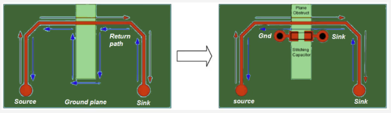
Split Ground Planes: Separating Analog and Digital Grounds
In mixed-signal PCBs, digital and analog circuits often coexist, but their grounding needs are different. Digital circuits generate fast-switching noise, while analog circuits require a quiet, stable ground. Split ground planes address this by physically separating the ground for digital and analog sections on the PCB.
For instance, in a PCB with an analog-to-digital converter (ADC), you might have one ground plane for the digital logic and another for the analog input circuitry. These planes are typically connected at a single point, often near the ADC, to provide a common reference without allowing noise to cross over.
While split ground planes can be effective, they must be designed with care. Incorrectly splitting planes or connecting them at multiple points can create ground loops and worsen noise. Always ensure return paths are considered when implementing this strategy.
Chassis Ground: Connecting to the Physical World
Chassis ground refers to connecting the PCB ground to the metal enclosure or chassis of your device. This type of grounding is crucial for safety, as it provides a path for fault currents to flow, protecting users from electric shock. It also helps shield the circuit from external EMI by creating a Faraday cage effect with the enclosure.
In practice, chassis ground is often connected to the PCB ground at a single point, usually near the power entry. For example, in an industrial control system, the chassis ground ensures that any static discharge or external interference is diverted away from sensitive components.
Always use a dedicated connection for chassis ground and avoid mixing it with signal grounds to prevent noise coupling. Additionally, ensure compliance with safety standards when implementing this strategy.
Digital Ground vs. Analog Ground: Managing Mixed Signals
As mentioned earlier, digital and analog grounds serve different purposes in mixed-signal designs. Digital ground handles the noisy, fast-switching currents of digital components like microcontrollers and logic gates. Analog ground, on the other hand, supports sensitive circuits like amplifiers and sensors, where even small noise levels (as low as 1 mV) can degrade performance.
The best practice is to separate these grounds physically on the PCB, using techniques like split ground planes or star grounding. Connect them at a single point to maintain a common reference without allowing digital noise to interfere with analog signals. For example, in an audio processing board, keeping digital and analog grounds separate can prevent clicks and pops in the output.
Pay close attention to component placement as well. Keep digital components away from analog sections to minimize crosstalk through the board or air.
Practical Tips for Effective PCB Grounding
Now that we've covered the main grounding strategies, here are some practical tips to apply them effectively in your PCB layouts:
- Minimize Return Path Lengths: Always route signals close to their ground return path to reduce loop area and impedance. For high-speed signals, this can mean placing ground vias next to signal vias.
- Use Ground Vias Wisely: In multi-layer boards, use multiple vias to connect components to the ground plane. This reduces impedance and ensures a solid connection.
- Avoid Ground Loops: Be mindful of creating multiple ground paths that can form loops. Stick to a single reference point or a well-designed ground plane.
- Consider Frequency: Low-frequency designs can use single point grounding, while high-frequency designs (above 10 MHz) benefit from multi-point grounding and ground planes.
- Test and Iterate: After designing your PCB, test for noise and interference. Use an oscilloscope to check for ground bounce or signal distortion, and adjust your grounding if needed.
Common Grounding Mistakes to Avoid
Even with the best intentions, grounding mistakes can creep into your design. Here are some common pitfalls and how to avoid them:
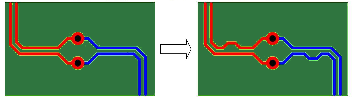
- Splitting Ground Planes Incorrectly: Avoid splitting ground planes under high-speed signal traces, as this can disrupt return paths and increase EMI.
- Long Ground Traces: Long traces increase impedance and can act as antennas, picking up noise. Keep ground connections short and direct.
- Ignoring Component Placement: Placing noisy digital components near sensitive analog circuits can lead to crosstalk. Plan your layout to separate these sections.
- Overlooking Chassis Ground: Failing to connect to chassis ground can leave your circuit vulnerable to external interference and safety hazards.
Conclusion: Building a Solid Foundation with PCB Grounding
Effective grounding is the foundation of a quiet, reliable PCB layout. Whether you're using single point grounding for a simple circuit or implementing split ground planes for a mixed-signal design, the right strategy can make all the difference in reducing noise and ensuring performance. By understanding concepts like ground planes, star grounding, multi-point grounding, chassis ground, digital ground, and analog ground, you can tackle a wide range of design challenges with confidence.
Start small by applying these techniques in your next project, and pay attention to how they impact noise and signal integrity. With practice, you'll develop an intuitive sense for grounding that will elevate the quality of your PCB designs. Remember, a well-grounded circuit is a quiet circuit, and quiet circuits lead to better results.