 ALLPCB


Designing a printed circuit board (PCB) as a hobbyist can be exciting, but it comes with challenges like determining the right trace width. If you're wondering how to calculate PCB trace width for your project, you're in the right place. This guide will walk you through the process step by step, focusing on key factors like current, temperature rise, and copper thickness. By the end, you'll know how to use the IPC-2221 standard, online calculators, and practical tips to ensure your PCB design is safe and efficient.
Whether you're building a simple LED circuit or a complex microcontroller board, understanding PCB trace width calculation is crucial to avoid overheating or failure. Let’s dive into this tutorial tailored for hobbyists, breaking down complex concepts into easy-to-follow steps.
Why PCB Trace Width Matters for Hobbyists
PCB trace width refers to the width of the copper paths on your board that carry electrical current. If the trace is too narrow for the current it carries, it can overheat, leading to potential damage or even a fire hazard. On the other hand, overly wide traces waste valuable board space, making your design less efficient. For hobbyists, striking the right balance is key to creating functional and safe projects.
Calculating the correct trace width ensures your PCB can handle the current without exceeding a safe temperature rise. It also helps maintain signal integrity and prevents voltage drops. This guide will cover everything from the basics of current and temperature to using standards like IPC-2221 for accurate calculations.

Key Factors in PCB Trace Width Calculation
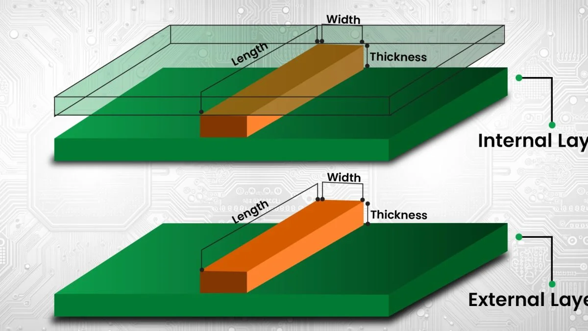
Before jumping into calculations, it’s important to understand the factors that influence trace width. These include current, temperature rise, copper thickness, and whether the trace is on an internal or external layer of the PCB. Let’s break each one down.
1. Current (Ampacity)
The amount of current (measured in amperes, or amps) that a trace needs to carry is the primary factor in determining its width. Higher currents require wider traces to prevent overheating. For example, a trace carrying 1 amp will need to be narrower than one carrying 5 amps, assuming all other factors are equal.
2. Temperature Rise
Temperature rise refers to how much hotter the trace gets compared to the surrounding environment when current flows through it. A common safe limit for hobbyist projects is a 10°C to 20°C rise. If the temperature rise is too high, it can damage components or the board itself. Your goal is to choose a trace width that keeps the temperature rise within acceptable limits.
3. Copper Thickness
Copper thickness, often measured in ounces per square foot (oz/ft2), affects how much current a trace can carry. Standard thicknesses for hobbyist PCBs are 1 oz/ft2 and 2 oz/ft2, which translate to about 35 micrometers and 70 micrometers, respectively. Thicker copper can handle more current for the same trace width, so it’s an important consideration.
4. Internal vs. External Traces
Traces on the outer layers of a PCB (external traces) dissipate heat better than those buried inside (internal traces). As a result, internal traces need to be wider to handle the same current compared to external ones. This is a critical factor if you’re designing a multilayer board.
Understanding the IPC-2221 Standard
The IPC-2221 standard is a widely accepted guideline for PCB design, including trace width calculations. It provides formulas and charts to determine the appropriate trace width based on current, temperature rise, and copper thickness. While newer standards like IPC-2152 exist, IPC-2221 remains popular among hobbyists due to its simplicity and availability in many online tools.
According to IPC-2221, the trace width can be calculated using a formula that considers the cross-sectional area of the copper trace. The general idea is to ensure the trace can carry the required current without exceeding a specified temperature rise. While the exact formula can be complex, online calculators simplify the process by doing the math for you.
Step-by-Step Guide to PCB Trace Width Calculation
Now that you understand the basics, let’s go through a step-by-step process to calculate PCB trace width. This tutorial is designed for hobbyists, so we’ll keep it practical and straightforward.
Step 1: Determine the Current
First, find out how much current your trace needs to carry. Check the specifications of the components or circuits connected to the trace. For example, if you’re powering a 5V LED strip that draws 2 amps, your trace must handle at least 2 amps of current.
Step 2: Set a Temperature Rise Limit
Decide on an acceptable temperature rise for your project. For most hobbyist applications, a 10°C to 20°C rise above ambient temperature (typically 25°C) is safe. If your project operates in a hotter environment or involves sensitive components, aim for a lower temperature rise, like 10°C.
Step 3: Identify Copper Thickness
Check the copper thickness of your PCB. If you’re ordering a board from a manufacturer, the default is often 1 oz/ft2 (about 35 micrometers). If you need higher current capacity, consider specifying 2 oz/ft2 during the design phase.
Step 4: Choose Internal or External Trace
Determine whether the trace will be on an internal or external layer. Remember that internal traces need to be wider due to poorer heat dissipation. If you’re working on a single- or double-layer board, your traces are likely external.
Step 5: Use an Online Calculator or Formula
For most hobbyists, using an online calculator based on IPC-2221 is the easiest way to find the right trace width. Many free tools are available on the web that allow you to input current, temperature rise, copper thickness, and layer type. The calculator will output the recommended trace width in millimeters or mils (thousandths of an inch).
If you prefer to calculate manually, the IPC-2221 formula for trace width is derived from empirical data. A simplified version for external traces is often expressed as:
Trace Width (mils) = (Current (amps) ^ 0.725) * k
Where 'k' is a constant based on temperature rise and copper thickness (typically around 0.048 for a 10°C rise with 1 oz/ft2 copper). However, since manual calculations can be error-prone, online tools are recommended for accuracy.
Step 6: Verify and Adjust
After calculating the trace width, double-check your inputs and results. If the calculated width seems too narrow or too wide for your board layout, adjust the parameters. For instance, increasing copper thickness or reducing temperature rise can allow for narrower traces. Also, ensure the width fits within your PCB design software’s manufacturing constraints, as very narrow traces may not be feasible for low-cost fabrication.
Practical Example: Calculating Trace Width for a 3-Amp Circuit
Let’s apply the steps to a real-world example. Suppose you’re designing a PCB for a motor controller that draws 3 amps at 12V. You want to keep the temperature rise below 15°C, and your board uses 1 oz/ft2 copper with external traces.
- Current: 3 amps
- Temperature Rise: 15°C
- Copper Thickness: 1 oz/ft2 (35 micrometers)
- Layer: External
Using an online calculator based on IPC-2221, you input these values. The result might suggest a trace width of approximately 1.5 mm (or 59 mils). This width ensures the trace can handle 3 amps without overheating beyond the 15°C limit.
If 1.5 mm is too wide for your layout, you could switch to 2 oz/ft2 copper, which might reduce the required width to around 0.8 mm (31 mils). Alternatively, if your design allows, you can add a heat sink or ventilation to lower the temperature rise requirement.
Using Online Calculators for PCB Trace Width
Online calculators are a lifesaver for hobbyists who want quick and accurate results without diving into complex formulas. These tools are often based on IPC-2221 or newer standards and account for variables like current, temperature rise, and copper thickness. Simply enter your parameters, and the tool provides the recommended trace width.
Some calculators also estimate additional factors like voltage drop and power loss, which can be helpful for optimizing your design. When choosing a calculator, look for one that allows flexible unit inputs (e.g., millimeters or mils) and clearly states the standard it uses for calculations.
Tips for Hobbyists to Optimize Trace Width in PCB Design
Beyond calculations, here are some practical tips to ensure your PCB design is safe and efficient:
- Leave Extra Space: If possible, make traces slightly wider than calculated to account for manufacturing tolerances or unexpected current spikes.
- Use Copper Pours: For high-current areas, consider using copper pours (large areas of copper) instead of narrow traces to improve heat dissipation.
- Check Manufacturer Limits: Ensure your trace width meets the minimum and maximum limits of your PCB manufacturer. Very narrow traces might increase costs or be prone to defects.
- Simulate Your Design: Use PCB design software with built-in simulation tools to verify that your traces won’t overheat under load.
- Account for Ambient Conditions: If your project will operate in a hot environment (e.g., outdoors in summer), aim for a lower temperature rise to compensate.
Common Mistakes to Avoid in Trace Width Calculation
As a hobbyist, it’s easy to make errors when calculating trace width. Here are some pitfalls to watch out for:
- Ignoring Temperature Rise: Assuming any trace width will work without considering heat buildup can lead to board failure.
- Forgetting Layer Type: Failing to account for whether a trace is internal or external can result in incorrect widths and overheating.
- Using Incorrect Copper Thickness: Double-check the copper weight of your board, as using the wrong value in calculations will skew results.
- Overloading Traces: Don’t push traces to their maximum current capacity for long periods; leave some margin for safety.
Conclusion: Mastering PCB Trace Width for Your Projects
Calculating PCB trace width doesn’t have to be intimidating, even for hobbyists. By understanding the roles of current, temperature rise, copper thickness, and layer type, you can design boards that are both safe and efficient. The IPC-2221 standard provides a reliable foundation, and online calculators make the process accessible to everyone.
Start with the step-by-step guide in this tutorial, use the practical example as a reference, and apply the tips to optimize your designs. With practice, you’ll gain confidence in handling trace width calculations for any project, from simple circuits to complex multilayer boards. Keep experimenting, and enjoy the process of bringing your electronic ideas to life!


