ALLPCB


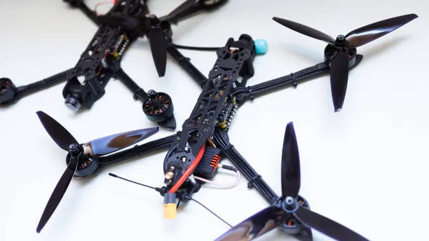
Designing a printed circuit board (PCB) for drones requires careful attention to trace routing to ensure both signal integrity and efficient power delivery. Whether you're working on a small hobby drone or a professional-grade unmanned aerial vehicle (UAV), optimizing your PCB layout can significantly impact performance, reliability, and flight efficiency. In this comprehensive guide, we'll explore key strategies for drone PCB trace routing, focusing on critical aspects like trace width calculation, impedance matching, differential pairs, star grounding, and current carrying capacity. By the end of this post, you'll have actionable insights to create high-performing drone PCBs that meet the demands of modern aerial systems.
Why Trace Routing Matters in Drone PCB Design
Trace routing in a drone PCB is more than just connecting components; it's about ensuring that signals travel without interference and power is delivered efficiently to motors, sensors, and control systems. Drones operate in dynamic environments where high-speed signals from sensors and communication modules must remain clear, and power delivery to motors must handle high currents without overheating or voltage drops. Poor trace routing can lead to issues like signal noise, electromagnetic interference (EMI), or even component failure, all of which can compromise a drone's performance or cause crashes.
In the following sections, we'll break down specific strategies to optimize trace routing for signal integrity and power delivery, tailored to the unique challenges of drone design.
1. Trace Width Calculation: Balancing Current and Space
One of the first steps in drone PCB design is determining the correct trace width for your circuits. Trace width calculation is crucial for ensuring that traces can handle the required current without overheating, while also fitting within the compact layout of a drone PCB. Too narrow traces can lead to excessive heat and potential failure, while overly wide traces waste valuable board space.
To calculate trace width, you need to consider the current carrying capacity and the temperature rise you're willing to accept. A common guideline is to use a trace width calculator based on industry standards like IPC-2221. For example, a trace carrying 2 amps of current on a standard 1 oz copper layer might require a width of approximately 50 mils (1.27 mm) to keep temperature rise below 10°C. For higher currents, such as those needed for drone motor power lines (often 5-10 amps or more), trace widths may need to be 100 mils or wider, or you might consider using thicker copper layers (e.g., 2 oz or 3 oz) to reduce resistance.
Additionally, ensure that power traces are as short and direct as possible to minimize voltage drops. For compact drone designs, where space is limited, prioritize wider traces for high-current paths and use vias or multiple layers if needed to maintain a clean layout.
2. Impedance Matching: Ensuring Signal Clarity
Impedance matching is a critical factor in maintaining signal integrity, especially for high-speed signals in drone PCBs. Drones often rely on fast communication protocols like I2C, SPI, or UART for sensor data and control signals, and mismatched impedance can cause signal reflections, leading to data errors or delays. For instance, a typical high-speed signal line might require a controlled impedance of 50 ohms for single-ended traces or 100 ohms for differential pairs.
To achieve impedance matching, you must design trace widths and spacing based on the dielectric constant of your PCB material and the layer stack-up. For example, on a standard FR-4 substrate with a dielectric constant of about 4.5, a 50-ohm trace on a 1.6 mm thick board might need a width of around 6 mils with specific ground plane spacing. Use simulation tools or impedance calculators to fine-tune these values during the design phase. Additionally, avoid sharp bends in high-speed traces—opt for 45-degree angles or smooth curves to prevent signal reflections.
For drone designs, where weight and size are critical, achieving impedance matching can be challenging due to limited layer counts. In such cases, prioritize critical high-speed lines and place them away from noisy power traces to reduce interference.
3. Differential Pairs: Minimizing Noise in High-Speed Signals
Differential pairs are widely used in drone PCBs for high-speed data transmission, such as in communication between flight controllers and sensors or for video feeds. These pairs consist of two traces carrying complementary signals, which helps cancel out noise and reduce EMI. However, improper routing of differential pairs can negate these benefits.
When routing differential pairs, keep the traces as close together as possible to maintain consistent coupling, but ensure they are spaced appropriately from other signals to avoid crosstalk. A common rule of thumb is to keep the spacing between the pair traces at least three times smaller than the spacing to adjacent traces. For example, if your differential pair traces are 5 mils apart, keep them at least 15 mils away from other signals. Also, ensure both traces in the pair are of equal length to prevent timing skew—differences as small as 10 mils can cause issues at high frequencies (e.g., above 100 MHz).
In drone PCBs, where space is tight, routing differential pairs often requires careful planning. Use inner layers for these signals if possible, and place ground planes nearby to provide a stable return path. This approach helps maintain signal integrity even in the noisy environment of a drone, where motors and power lines can introduce significant interference.
4. Star Grounding: Reducing Noise and Ground Loops
Grounding is a fundamental aspect of PCB design, and in drones, where multiple systems (motors, sensors, and controllers) share the same board, a poor grounding strategy can lead to noise and ground loops. Star grounding is an effective technique to minimize these issues by connecting all ground points to a single central ground node, rather than daisy-chaining them across the board.
In a star grounding layout, each subsystem—such as the flight controller, motor drivers, and sensors—has its own dedicated ground trace that connects directly to the central ground point, often near the main power input. This prevents high-current returns from motors from interfering with sensitive analog or digital signals. For example, a drone with four motors might have separate ground traces for each motor driver, all meeting at a single ground pad near the battery connector, ensuring clean signal paths for the flight controller.
In practice, implementing star grounding in a compact drone PCB can be tricky due to space constraints. If a pure star configuration isn't feasible, consider using a ground plane with strategic cuts or splits to isolate noisy and quiet areas. Just ensure that return currents for high-power components don't cross sensitive signal areas.
5. Current Carrying Capacity: Handling High Power Demands
Drones often require significant power for motors, which can draw currents ranging from 5 to 20 amps or more per motor during peak operation. Ensuring that your PCB traces can handle this current carrying capacity is essential to prevent overheating, voltage drops, or trace burnout. As mentioned in the trace width section, wider traces and thicker copper layers are key to managing high currents.
Beyond trace width, consider the placement of power traces to optimize current flow. Keep power traces short and direct, and avoid routing them near sensitive signal lines to prevent EMI. For high-current paths, you might also use multiple vias to connect traces across layers, effectively increasing the cross-sectional area and reducing resistance. For instance, a power trace for a drone motor rated at 15 amps might use a 2 oz copper layer with a width of 150 mils, supplemented by 10 vias if it crosses layers, to ensure reliable current delivery.
Thermal management is another factor to consider. High currents generate heat, and in a drone, where airflow might be limited, this can lead to hotspots. Add thermal reliefs or copper pours around high-current areas to dissipate heat, and consider placing power components near the board edges for better cooling during flight.
Additional Tips for Drone PCB Trace Routing
Beyond the core strategies discussed, here are a few additional tips to enhance your drone PCB design:
- Layer Management: Use multiple layers to separate power, ground, and signal traces. A typical 4-layer board might dedicate the top and bottom layers to signals, with inner layers for power and ground planes.
- Component Placement: Place high-current components like motor drivers close to power inputs to minimize trace lengths. Similarly, position sensitive components like gyroscopes away from noisy areas.
- Simulation and Testing: Use PCB design software with simulation features to test signal integrity and power delivery before manufacturing. Post-production testing with real-world flight conditions can also reveal hidden issues.
Challenges in Drone PCB Routing and How to Overcome Them
Drone PCB design comes with unique challenges due to size, weight, and performance constraints. Limited board space often forces designers to compromise on trace spacing or layer count, while the need for lightweight designs can restrict the use of thicker copper or additional layers. Additionally, the high-vibration environment of a drone can stress solder joints and traces, leading to failures over time.
To address these challenges, prioritize critical traces (e.g., high-speed signals and high-current paths) during routing, and use compact components to save space. Reinforce mechanical stability by adding mounting holes or adhesive under critical components, and consider flexible PCB materials for areas prone to vibration. Finally, iterate your design with prototypes to identify and fix issues before mass production.
Conclusion: Building Better Drone PCBs with Optimized Trace Routing
Effective trace routing is the backbone of a high-performing drone PCB. By focusing on strategies like trace width calculation, impedance matching, differential pairs, star grounding, and current carrying capacity, you can ensure that your drone operates reliably under demanding conditions. Whether you're designing for hobby projects or commercial applications, these techniques will help you achieve superior signal integrity and power delivery, leading to smoother flights and longer-lasting hardware.
Start by applying these principles in your next drone PCB project, and remember that every design is an opportunity to refine your skills. With careful planning and attention to detail, you can create PCBs that meet the rigorous demands of modern drone technology.