In the world of PCB manufacturing, ensuring that your board can be tested efficiently is just as important as designing for functionality. This is where design for testability ICT (In-Circuit Testing) comes into play. By optimizing your PCB layout for ICT, you can reduce testing costs, improve defect detection, and speed up production. But how do you achieve this? The key lies in strategic planning, such as following test point placement guidelines, ensuring proper ICT probe access, and focusing on minimizing ICT fixture costs. In this comprehensive guide, we’ll walk you through the essential steps and best practices to design a PCB that’s ready for efficient in-circuit testing.
What is In-Circuit Testing (ICT) and Why Does It Matter?
In-Circuit Testing, or ICT, is a widely used method in electronics manufacturing to test individual components and connections on a printed circuit board (PCB) without powering up the entire system. It uses a bed-of-nails fixture—a setup with numerous probes that make contact with specific points on the PCB—to check for shorts, opens, and component values like resistance, capacitance, and more. ICT is critical because it helps catch manufacturing defects early, saving time and money in the production process.
Designing for ICT isn’t just an afterthought; it’s a proactive approach that can impact up to 25-30% of the total production cost, which is often attributed to testing. A well-thought-out design ensures that testing is faster, more accurate, and less expensive. Let’s dive into how you can optimize your PCB layout to achieve these benefits.
Key Principles of Design for Testability (DFT) in ICT
Before we get into specific layout strategies, it’s important to understand the core principles of design for testability ICT. DFT focuses on making a PCB easier to test by planning ahead during the design phase. Here are the foundational ideas:
- Accessibility: Ensure that test probes can physically reach the necessary points on the board without obstruction.
- Coverage: Maximize the number of nets (connections) that can be tested to catch as many defects as possible.
- Cost Efficiency: Design in a way that reduces the complexity and cost of test fixtures.
- Reliability: Avoid designs that could lead to false test failures due to poor contact or interference.
With these principles in mind, let’s explore actionable strategies for optimizing your PCB layout for ICT.
1. Test Point Placement Guidelines for Effective ICT
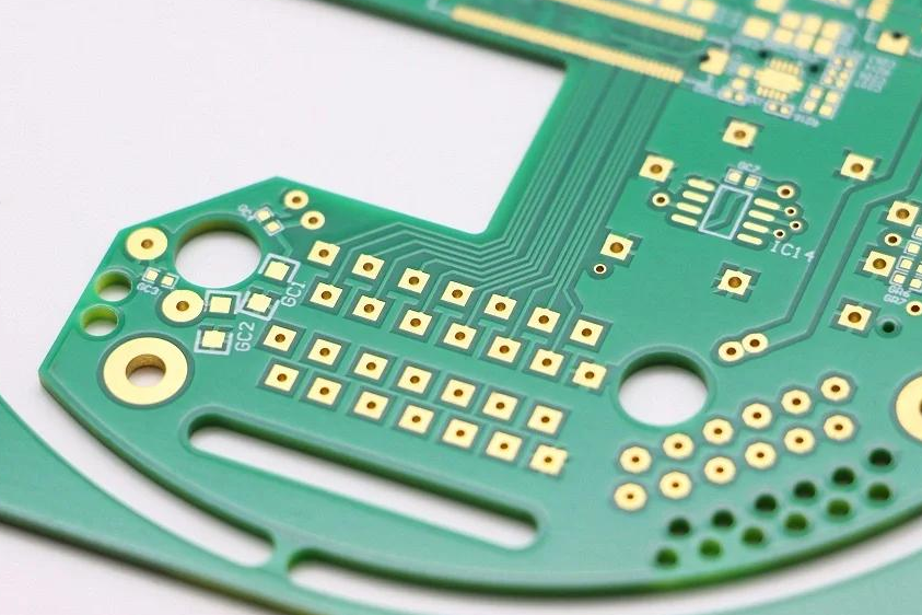
One of the most critical aspects of designing for ICT is following test point placement guidelines. Test points are specific locations on the PCB where probes make contact during testing. Poorly placed test points can lead to incomplete testing or increased fixture costs. Here are some best practices:
- Place Test Points on Every Net: Ideally, each net (a connection between components) should have at least one accessible test point. This ensures maximum test coverage. For a typical PCB with 500 nets, aim for at least 80-90% coverage, meaning 400-450 nets should have test points.
- Use Consistent Pad Sizes: Test points should have uniform pad sizes, typically between 0.8 mm to 1.2 mm in diameter, to ensure reliable probe contact. Smaller pads can lead to misalignment, while larger ones waste valuable board space.
- Maintain Clearances: Keep a minimum clearance of 2.5 mm between test points to avoid probe interference. Also, ensure test points are at least 3 mm away from tall components like capacitors or connectors to prevent physical obstruction.
- Distribute Evenly: Avoid clustering test points in one area of the board. Spread them out to balance the pressure on the test fixture and reduce the risk of bending or damage during testing.
2. Optimizing PCB Layout for ICT Probe Access
Ensuring proper ICT probe access is another cornerstone of a testable PCB design. If probes can’t reach the test points due to component placement or board layout, the testing process becomes inefficient or even impossible. Follow these tips to improve access:
- Single-Sided Access: Whenever possible, place all test points on one side of the PCB (usually the bottom side). Dual-sided probing increases fixture complexity and costs by requiring probes on both sides. For instance, a single-sided fixture might cost around $1,500, while a dual-sided one could exceed $2,500 for the same board.
- Avoid Obstructions: Keep test points away from areas under large components, such as heat sinks or tall electrolytic capacitors, which can block probe access. If unavoidable, consider using through-hole vias as test points, ensuring they are not covered by solder mask.
- Tooling Holes for Alignment: Include at least two non-plated tooling holes (preferably three) on opposite diagonal corners of the PCB. These holes, typically 3.2 mm in diameter, help align the board precisely with the test fixture, ensuring accurate probe contact. Misalignment by even 0.1 mm can lead to test failures.
3. Component Placement Strategies for ICT Compatibility
The way you place components on your PCB can significantly impact its testability. A cluttered or poorly organized layout can hinder probe access and increase testing challenges. Here’s how to optimize component placement for ICT:
- Group Similar Components: Place components of the same type (e.g., resistors, capacitors) in clusters with consistent orientation. This not only simplifies assembly but also makes it easier to design test fixtures with uniform probe patterns.
- Keep Test Areas Clear: Reserve space around test points by avoiding nearby component placement. For example, maintain a 5 mm keep-out zone around critical test points for high-voltage nets to prevent accidental probe contact with adjacent parts.
- Minimize Component Height Near Test Points: Tall components can cast shadows or physically block probes. If a component must be near a test point, ensure its height is under 6 mm to allow probe access from standard fixture angles (typically 90 degrees).
By planning component placement early in the design process, you can avoid costly redesigns and ensure a smoother testing phase.
4. Minimizing ICT Fixture Costs Through Smart Design
One of the biggest expenses in ICT is the cost of the test fixture itself. A bed-of-nails fixture can range from $1,000 to $5,000 or more, depending on the complexity of the PCB. Here are proven strategies for minimizing ICT fixture costs:
- Reduce Probe Count: While it’s ideal to test every net, prioritize critical nets (e.g., power, ground, and high-speed signals) if board space is limited. Reducing the number of probes by even 10% can cut fixture costs significantly. For a board requiring 500 probes, dropping to 450 could save hundreds of dollars.
- Standardize Probe Types: Use standard probe sizes and types (e.g., 100-mil spacing probes) rather than custom ones. Custom probes can increase fixture costs by 20-30% due to specialized manufacturing.
- Simplify Fixture Design: Avoid designs that require vacuum or pneumatic fixtures unless absolutely necessary, as these add to the cost and maintenance. A basic mechanical fixture is often sufficient for boards with fewer than 1,000 test points.
5. Addressing Signal Integrity in ICT Design
While focusing on testability, don’t overlook signal integrity, especially for high-speed or sensitive circuits. Poor test point placement or excessive probing can introduce noise or affect performance. Consider these points:
- Avoid High-Speed Nets: If possible, avoid placing test points directly on high-speed signal traces (e.g., traces with frequencies above 100 MHz). The added capacitance from a test point can degrade signal quality. Instead, use nearby vias or less critical points for testing.
- Ground Test Points: Ensure that ground test points are placed near power test points to provide a stable reference during testing. A typical ratio is one ground test point for every five power or signal test points.
- Minimize Stub Lengths: Keep test point stubs (extra trace length leading to the test point) under 5 mm to reduce signal reflection and interference, especially for impedance-controlled traces targeting 50 ohms.
Balancing testability with signal integrity ensures that your PCB performs well both during testing and in its final application.
6. Common Mistakes to Avoid in PCB Layout for ICT
Even with the best intentions, certain design oversights can undermine ICT effectiveness. Here are common pitfalls and how to avoid them:
- Ignoring Test Point Accessibility: Placing test points under components or in crowded areas can render them useless. Always double-check accessibility during layout reviews.
- Overloading One Side: Clustering all test points on a small section of the board can strain the fixture and lead to uneven probe pressure. Distribute them evenly across the board surface.
- Forgetting Tooling Holes: Without proper alignment holes, fixtures can’t position the board accurately, leading to missed probes and false test results. Always include them in your design.
- Neglecting Documentation: Failing to provide clear test point and net information to the manufacturer can delay fixture design. Include a detailed test point map in your design files.
By steering clear of these mistakes, you can save time and resources during the testing phase.
7. Tools and Software for ICT-Friendly PCB Design
Modern PCB design software offers features to help with design for testability ICT. While specific tool names vary, look for these capabilities in your design platform:
- Test Point Assignment: Automatically assign test points to nets based on coverage goals, saving manual effort.
- Clearance Checks: Validate test point spacing and keep-out zones to ensure probe access.
- Fixture Simulation: Simulate fixture alignment and probe contact to identify potential issues before manufacturing.
Using these tools can streamline the process of creating an ICT-ready layout, reducing errors and improving efficiency.
Conclusion: Building Testability Into Your PCB Design
Designing a PCB with in-circuit testability in mind is a smart investment that pays off in reduced costs, faster production, and higher product quality. By following test point placement guidelines, ensuring proper ICT probe access, and focusing on minimizing ICT fixture costs, you can create a PCB layout for ICT that meets both manufacturing and testing needs. Remember to prioritize accessibility, balance test coverage with signal integrity, and avoid common design pitfalls.
Start incorporating these design for testability ICT strategies into your next project. With careful planning and attention to detail, you’ll not only streamline the testing process but also deliver reliable, high-quality boards ready for the market. If you’re looking for a trusted partner to bring your ICT-optimized designs to life, our team is here to support you every step of the way.
 ALLPCB


